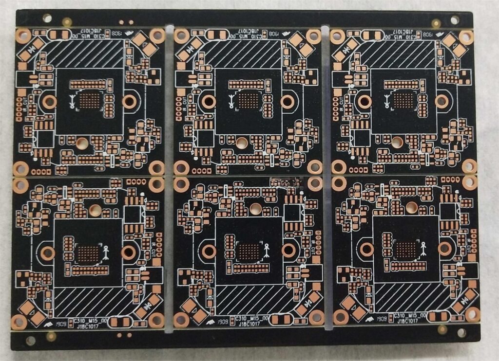
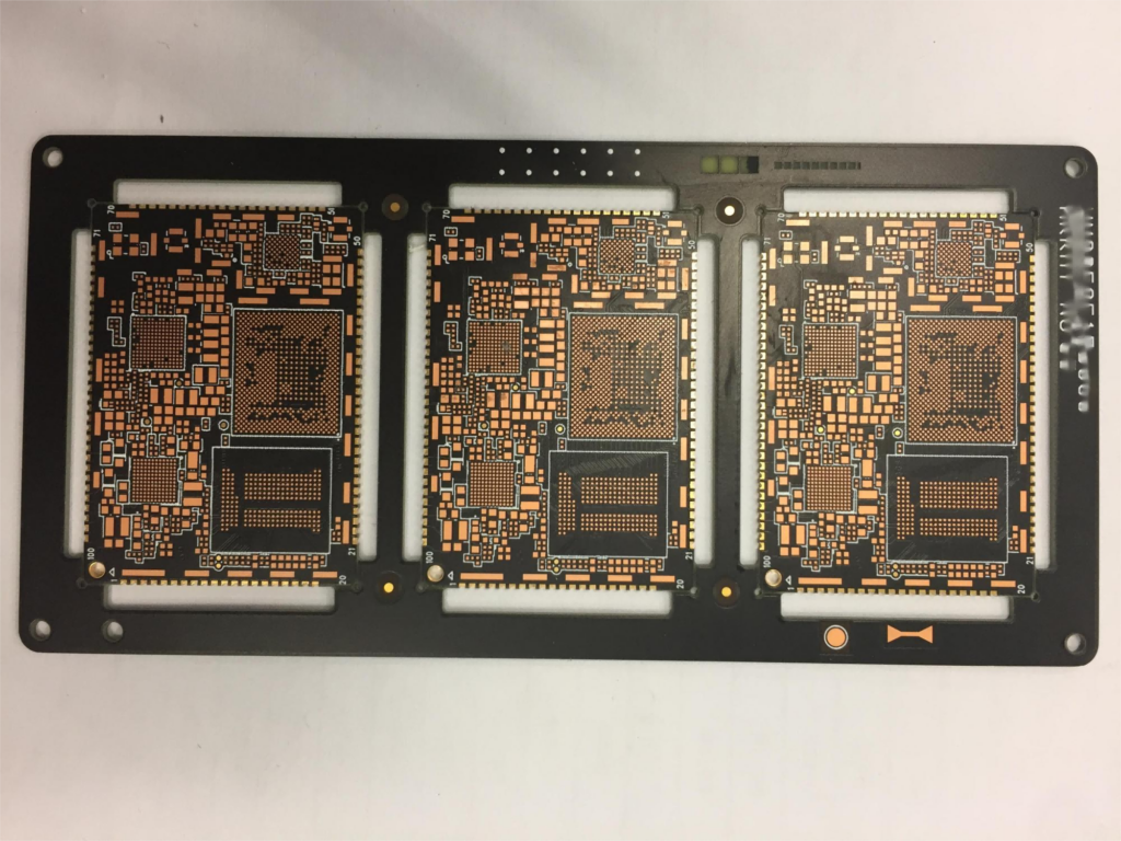
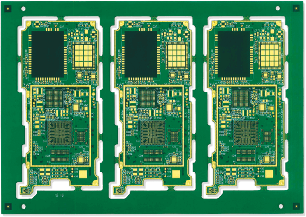
Fumax — Special contract manufacturer of HDI PCBs in Shenzhen. Fumax offers the full range of technologies, from 4-layer laser to 6-n-6 HDI multilayer in all thicknesses. Fumax is good at manufacturing high technology HDI(High Density Interconnection)PCBs. Products include large and thick HDI boards and high density thin stacked micro via constructions. HDI technology enables PCB layout for very high density components like 400um pitch BGA with a high amount of I/O pins. This type component usually requires a PCB board using multiple layer HDI, for example 4+4b+4. We have years experience for manufacturing this kind of HDI PCBs.
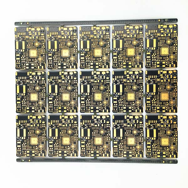
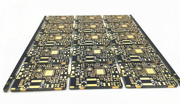
The product range of HDI PCB that Fumax can offer:
* Edge plating for shielding and ground connection;
* Copper-filled micro vias;
* Stacked and staggered micro vias;
* Cavities, countersunk holes or depth milling;
* Solder resist in black, blue, green, etc.
* Minimum track width and spacing in mass production around 50μm;
* Low-halogen material in standard and high Tg range;
* Low-DK Material for Mobile Devices;
* All recognised printed circuit board industry surfaces available.
Competence:
* Material Type(FR4 / Taconic / Rogers / Others on Request);
* Layer(4 – 24 Layers);
* PCB Thickness Range(0.32 – 2.4 mm);
* Laser Technology(CO2 Direct Drilling (UV/CO2));
* Copper Thickness(9µm / 12µm / 18µm / 35µm / 70µm / 105µm);
* Min. Line / Spacing(40µm / 40µm);
* Max. PCB Size(575 mm x 500 mm);
* Smallest Drill(0.15 mm).
* Surfaces(OSP / Immersion Tin/NI/Au/Ag、Plated Ni/Au).
Applications:
High Density Interconnects (HDI) board are a board (PCB) with a higher wiring density per unit area than normal printed circuit boards (PCB). HDI PCB have smaller lines and spaces (<99 µm), smaller vias (<149 µm) and capture pads (<390 µm), I/O>400, and higher connection pad density (>21 pads/sq cm) than employed in conventional PCB technology. HDI board can reduce size and weight, as well as to enhance the whole PCB electrical performance. As consumer demands change, so must technology. By using HDI technology, designers now have the option to place more components on both sides of the raw PCB. Multiple via processes, including via in pad and blind via technology, allow designers more PCB real estate to place components that are smaller even closer together. Decreased component size and pitch allow for more I/O in smaller geometries. This means faster transmission of signals and a significant reduction in signal loss and crossing delays.
* Automotive Products
* Consumer Electronic
* Industrial Equipment
* Medical Appliance Electronics
* Telecom Electronics
