With the continuous development of technology, display screens are increasingly used in many fields, such as smart homes, medical equipment, industrial automation, etc.
In order to meet customers’ individual needs for display PCB assembly, customized display PCB assembly projects came into being.
This article will introduce in detail all aspects of the custom display PCB assembly project, including project background, demand analysis, solution design, implementation process, advantages and case applications, etc.
Background of the project
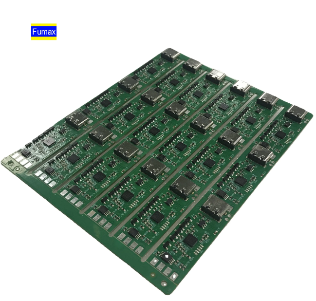
As an important medium for human-computer interaction, display screens play a vital role in modern society. As one of the core components of the display screen, PCB (Printed Circuit Board) carries various electronic components and is responsible for signal transmission and processing.
Due to the different application requirements of display screens in different fields, traditional standardized PCB assembly solutions can no longer meet market demand. Therefore, the customized display PCB assembly project came into being, aiming to provide customers with personalized and customized PCB assembly services to meet their special needs.
Demand analysis
In a custom display PCB assembly project, demand analysis is a crucial part. First of all, the project team needs to have in-depth communication with the customer to understand their specific needs for display PCB, such as size, thickness, weight, interface type, display resolution, etc. Secondly, the project team also needs to consider the working environment and usage scenarios of the display PCB to ensure that the designed PCB can adapt to various harsh environments, such as high temperature, low temperature, high humidity, etc. Finally, the project team also needs to quantify and refine the customer’s needs to provide a basis for subsequent program design and implementation.
Design
After understanding the customer’s needs, the project team needs to start designing a custom display PCB assembly solution. Solution design includes PCB layout design, electronic component selection, production process planning, test plan formulation, etc. In terms of layout design, the project team needs to reasonably plan the layout and routing of electronic components based on the customer’s needs and the actual size of the PCB to ensure the performance and stability of the PCB.
In terms of electronic component selection, the project team needs to select appropriate electronic components based on the customer’s needs and working environment to ensure their quality and performance. In terms of production process planning, the project team needs to develop detailed production process flow and quality control standards to ensure that the PCB produced meets customer requirements.
In terms of test plan formulation, the project team needs to design a comprehensive test plan, including electrical performance testing, functional testing, environmental adaptability testing, etc., to ensure the stability and reliability of the PCB.
Implementation process
After the solution design is completed, the project team needs to start implementing the custom display PCB assembly project. The implementation process includes raw material procurement, PCB production, component welding, testing and inspection, packaging and delivery.
In the raw material procurement process, the project team needs to purchase according to the component list in the design document to ensure that the quality and performance of the components meet the design requirements. In the PCB production process, advanced production equipment and technology need to be used to produce PCB boards that meet design requirements.
In the component welding process, professional welding equipment and operators need to be used to complete the component welding work. In the testing and inspection process, comprehensive testing and inspection work is required to ensure that each PCB meets the design requirements and quality standards.
In the packaging and delivery process, the product needs to be properly packaged and labeled, and delivered in the manner required by the customer.
Advantage analysis
Customized display PCB assembly projects have the following advantages:
- Personalized customization: Personalized customization according to the needs of customers to meet their special needs.
- High-quality products: Adopt advanced production technology and strict quality control system to ensure that product quality and performance meet customer requirements.
- Professional technical support: We have a professional technical support team that can provide customers with technical consultation, solutions, technical support and other services.
- Quick response: It has flexible supply chain management capabilities and can quickly respond to customer needs to ensure timely supply of products.
Case Application
Customized display PCB assembly projects are widely used in various fields.
For example, in the field of smart home, customized display PCB can be used as the control core of smart speakers, smart door locks and other equipment; in the field of medical equipment, customized display PCB can be used in the display and control part of medical equipment; in the field of industrial automation , customized display PCB can be used in industrial robot control systems, etc. These cases demonstrate the wide application and importance of custom display PCB assembly projects in various fields.
Summary and Outlook
As a personalized and customized service solution, the customized display PCB assembly project provides customers with more flexible and diverse choices.
By in-depth understanding of customer needs, designing personalized solutions, using advanced technology and strict quality control, customized display PCB assembly projects can provide customers with high-quality, high-performance display PCB products.
With the continuous development of technology and changing market demands, customized display PCB assembly projects will face more challenges and opportunities.
In the future, the project team needs to continuously innovate and optimize service solutions, improve technical level and production capacity, to better meet customer needs and promote the development of the industry.