Differences in ceramic PCB gold plating manufacturing process
The gold plating processes on ceramic PCB mainly include hard gold, soft gold, electroplated gold, chemical gold and flash gold. The ceramic circuit board manufacturing process is different.
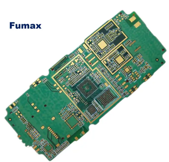
Fumax is a one-stop electronic manufacturing service in China that focuses on high-speed PCB design, ceramic PCB circuit board manufacturing, ceramic PCB processing, and SMT patch assembly.
The difference between hard gold plating, soft gold plating, electroplating gold, chemical gold and flash gold on ceramic PCB
The gold plating processes on ceramic PCB mainly include hard gold, soft gold, electroplated gold, chemical gold and flash gold. The following are the main differences between these processes:
- Hard gold: Hard gold is a process in which gold particles are attached to the PCB board through electroplating. It has the advantages of strong adhesion, good wear resistance, and resistance to plugging and unplugging. Therefore, it is often used to make electronic components that are pluggable and touch-resistant, such as gold fingers, calculator boards, etc.
- Soft gold: Soft gold is a process that attaches gold particles to the PCB board through a chemical reaction. It has the advantages of weak adhesion and easy soldering, so it is often used to make electronic components that require wiring or welding, such as gold fingers of memory modules.
- Gold electroplating: Gold electroplating is a process in which gold ions are reduced into metal and deposited on the PCB board through electroplating. It has the advantages of strong adhesion, good conductivity, and corrosion resistance, so it is often used to make high-precision electronic components, such as mobile phone circuit boards.
- Gold formation: Gold formation is a process that uses a chemical reaction to reduce gold ions into metal and deposit it on the PCB board. It has the advantages of weak adhesion and easy tinning, so it is often used to make electronic components that require wiring or welding, such as calculator boards.
- Flash gold: Flash gold is a process that uses a special process to cover the surface of the PCB board with a layer of metal particles. It has the advantages of beautiful appearance, wear resistance and corrosion resistance, so it is often used to make high-end electronic components or decorations.
In short, different gold plating processes have different characteristics and application areas, and the appropriate process needs to be selected according to specific needs.
Can you explain in detail why hard gold has strong adhesion?
The reason for the strong adhesion of hard gold is mainly due to the electroplating process used in its production process, which allows the gold particles to adhere closely to the surface of the PCB board. Specifically, the production process of hard gold includes the following steps:
- Pretreatment: Before electroplating, the PCB board needs to be pretreated, including cleaning, drying and other steps to remove impurities and moisture on the surface and ensure the adhesion of gold plating.
- Gold electroplating: Gold particles are attached to the surface through electroplating on the pre-treated PCB board. In this process, the gold ions are reduced to metal under the action of electric current and deposited on the PCB board, forming a uniform and dense gold layer.
- Heat treatment: In order to improve the hardness and adhesion of gold, heat treatment is required. At high temperatures, the gold layer will undergo structural transformation to form a metallographic structure with high hardness, which will also make the gold layer and the surface of the PCB board more closely combined.
Since the electroplating process is used in the production of hard gold, the gold particles can adhere closely to the surface of the PCB board. In addition, the metallographic structure with high hardness formed after heat treatment makes the adhesion of hard gold strong. At the same time, hard gold also has the advantages of good wear resistance and resistance to insertion and removal, and is often used to make electronic components that are resistant to insertion and removal and touch.
What are the characteristics of PCB hard gold?
PCB hard gold has the following characteristics:
- High hardness: Hard gold has a higher hardness than traditional gold, and is more wear-resistant and less likely to deform.
- Light weight: Hard gold uses hollow nanotechnology, which is larger in size but lighter in weight, making it more comfortable to wear.
- Exquisite style: The style of hard gold jewelry is usually more exquisite, more three-dimensional and fashionable than traditional gold.
- Higher price: Because the processing technology of hard gold is more complex, the price is usually higher than that of traditional gold.
- Environmental protection: Hard gold uses advanced nanotechnology, which has less impact on the environment during the production process.
In general, hard gold has the characteristics of high hardness, light weight, exquisite style, high price and environmental protection. It is a gold jewelry with high added value.
What other uses are there for electronic components that are resistant to plugging, unplugging and touching?
In addition to being used to make electronic components, electronic components that are resistant to plugging, pulling, and touching can also be used to make various connectors, terminals, switches and other components that require frequent plugging or touching, such as USB connectors and headphone jacks. , power switch, etc. These components need to have high wear resistance and longevity to avoid damage caused by frequent plugging and unplugging or contact, thereby improving product reliability and user experience. In addition, electronic components that are resistant to plugging and unplugging and are resistant to touch can also be used to make products in medical devices, communication equipment, industrial control and other fields to meet the durability and stability requirements in specific environments.
In what aspects does PCB hard gold have good wear resistance?
The good wear resistance of PCB hard gold is mainly reflected in the following aspects:
- Surface hardness and wear resistance: PCB hard gold has high surface hardness and wear resistance, and can withstand greater friction and wear, thereby extending the service life of the PCB.
- Adhesion: PCB hard gold has strong adhesion to the base material and is not easy to fall off or crack, ensuring the stability and reliability of the PCB.
- Corrosion resistance: PCB hard gold has good corrosion resistance and can resist erosion by various chemical substances, thus ensuring the stability and reliability of PCB.
- Fatigue resistance: PCB hard gold has good fatigue resistance and can withstand repeated bending and twisting, thus ensuring the stability and reliability of the PCB.
In short, PCB hard gold has good wear resistance, adhesion, corrosion resistance and fatigue resistance, can meet the requirements of high precision and high reliability, and is widely used in electronics, communications, aerospace and other fields.
In the gold electroplating process, how are gold ions reduced to metal?
In the gold electroplating process, gold ions are reduced to metal through a reduction reaction. This reduction reaction is mainly under acidic conditions, through the action of electric current, the gold ions gain electrons and are reduced to metal. Specifically, the gold electroplating process includes the following steps:
- Preparation stage: A solution containing gold ions needs to be prepared as the electroplating solution, and an electrode, usually a metal anode, is needed to provide electrons.
- Electrification stage: Pass current into the prepared electroplating solution. Under the action of the current, gold ions will receive electrons and be reduced to metal, and deposited on the electrode surface.
- Deposition stage: As the deposition time prolongs, metal will gradually deposit on the electrode surface to form a metal layer.
- Removal stage: When the metal layer reaches a certain thickness, the electrode needs to be taken out and followed up, such as cleaning, drying, etc.
In the process of gold electroplating, the process of gold ions receiving electrons and being reduced to metal is a key step. This process is mainly affected by factors such as current density, plating solution composition and temperature. By controlling these factors, the thickness and quality of electroplated gold can be controlled. At the same time, in order to obtain a high-quality electroplated gold layer, appropriate pre- and post-processing are also required.
Can you explain in detail the reduction reaction process of gold ions during gold electroplating?
In the gold electroplating process, the reduction reaction process of gold ions is as follows:
- In an electroplating bath, a solution containing gold ions generates electric current through electrolysis.
- The anode (usually an inert electrode such as platinum or titanium) releases electrons under the influence of electric current, and these electrons move toward the cathode.
- The cathode (the substrate that needs to be electroplated, such as a PCB board) accepts these electrons and starts the reduction reaction.
- During the reduction process of gold ions, gold ions gain electrons from the solution and are reduced to metallic gold. This process is achieved through the action of electric current, which flows from the anode to the cathode, providing the necessary electrons for the reduction of gold ions.
- As time goes by, more gold ions gain electrons on the cathode and are reduced to metallic gold, forming an electroplated gold layer.
This process is part of an electrochemical reaction in which oxidation reactions at the anode and reduction reactions at the cathode occur simultaneously. By controlling parameters such as current density, electrolyte composition and temperature, the reduction process of gold ions can be affected, thereby controlling the thickness and quality of electroplated gold.
How do electrodes provide electrons during gold plating?
In the gold electroplating process, the electrodes provide the required electrons through the gain and loss of electrons. Specifically, when power is applied between the anode (platinum and titanium mesh) and the cathode (silicon wafer), the solution is energized and an electric field is formed. The anode undergoes an oxidation reaction to release electrons, while the cathode receives electrons and undergoes a reduction reaction. These electrons move directionally to the cathode through the action of the electric field, combine with gold ions in the solution, and accumulate on the surface of the silicon wafer in the form of gold atoms to form an electroplated gold layer. Therefore, the electrode promotes the redox reaction by providing electrons during the gold electroplating process, thereby achieving the deposition of the gold layer.
Can copper electroplating be used instead of gold electroplating?
In some cases, copper electroplating can be used instead of gold electroplating. The electroplated copper process has the advantages of low cost, strong adhesion, and good conductivity. Therefore, in some occasions where aesthetic requirements are not high, electroplated copper can be used instead of gold plating.
However, the electroplating gold process has advantages over electroplated copper in terms of aesthetics, corrosion resistance and electrical conductivity. In situations where high conductivity, high corrosion resistance and aesthetics are required, such as mobile phone circuit boards, memory sticks and other high-end electronic products, the electroplating process is still required.
Therefore, whether to use copper electroplating process to replace gold electroplating process needs to be decided according to the specific application scenarios and usage requirements. On the premise of meeting the usage requirements, priority should be given to processes with lower cost and better environmental protection.
In addition to gold plating, are there other surface treatment technologies used on PCBs?
In addition to gold plating, there are many other surface treatment technologies used on PCBs. These technologies include but are not limited to:
- Antioxidation treatment: By coating a layer of antioxidant film on the PCB surface, copper foil and other metal materials can be protected from oxidation and corrosion.
- Spray tin treatment: By coating the surface of the PCB with a layer of tin, the copper foil and other metal materials can be protected from oxidation and corrosion, and the welding performance of the PCB can also be improved.
- Lead-free tin spraying treatment: Compared with traditional lead-based tin spraying treatment, lead-free tin spraying treatment uses environmentally friendly lead-free materials, which is more in line with environmental protection requirements.
- Immersion gold treatment: By coating a layer of metallic gold on the PCB surface, the conductivity and corrosion resistance of the PCB can be improved.
- Immersion silver treatment: By coating a layer of metallic silver on the PCB surface, the conductivity and corrosion resistance of the PCB can be improved.
- Hard gold plating: By plating a layer of hard gold on the PCB surface, the hardness and corrosion resistance of the PCB can be improved.
- Full board gold plating: By plating a layer of metal gold or copper on the entire surface of the PCB, the conductivity and corrosion resistance of the PCB can be improved.
- Gold finger treatment: In equipment such as memory sticks, by plating a layer of metallic gold or copper on the connecting parts, the conductivity and corrosion resistance of the connecting parts can be improved.
These surface treatment technologies can be used alone or in combination as needed to meet the needs of different products.
The ceramic PCB gold plating manufacturing process is mainly divided into two types: chemical gold plating and electroplating gold plating.
- Chemical gold plating:
Electroless gold plating uses chemical methods to deposit a layer of nickel, palladium and gold on the surface of the copper layer of printed circuits. It is a non-selective surface processing process. The main process flow includes oil removal, micro-etching, pre-soaking, activation, nickel immersion, palladium immersion, gold immersion, drying and other links. There will be multi-level water washing between each link. The mechanism of chemical gold plating reaction mainly includes two types: redox reaction and displacement reaction. The advantage of this method is that it uses a leadless gold plating process to reduce the lead arrangement space and adapt to more precise and high-end electronic circuits. At the same time, the overall production cost of chemical gold plating is low. - Electroplating gold:
Gold plating is to attach gold particles to the PCB board through electroplating. Because of its strong adhesion, it is also called hard gold. In ceramic PCB prototyping, the use of this process can greatly increase the hardness and wear resistance of PCB, effectively prevent the diffusion of copper and other metals, and can adapt to the requirements of hot pressure welding and soldering.
In the ceramic PCB gold plating manufacturing process, chemical gold plating and electroplating gold plating have their own characteristics and advantages, and the appropriate process needs to be selected based on specific application scenarios and usage requirements.
Which ceramic PCB gold plating process manufacturer is the best in China?
Shenzhen fumax Technology Co., Ltd. focuses on ceramic circuit board PCBA design customization and PCB assembly services, one-stop services such as SMT patching, DIP welding, assembly testing and painting.
Fumax provides PCB and PCBA OEM/ODM services to global customers, specializing in the production of ceramic PCB boards, high-frequency PCB boards, ceramic copper-clad substrates, DPC ceramic substrates, DBC ceramic substrates, thick copper PCB boards, multi-layer PCB boards and SMT chip welding technology Service; is an influential ceramic PCB circuit board manufacturer in China.