What is PCB (printed circuit board) cloning?
PCB cloning or PCB copying is a common phenomenon in the electronics industry. It refers to the reverse research and development of existing physical electronic products and physical circuit boards, and the processing of technical files such as PCB files, bill of materials (BOM) files, schematic files, and PCB silk screen production files of the original products. 1:1 restoration, and then use these technical documents and production documents to perform PCB board manufacturing, component welding, flying probe testing, and circuit board debugging to complete a complete copy of the original circuit board model.
PCB cloning is not just a simple copy, it is a reverse research technology. Through PCB cloning, you can not only restore the circuit board 1:1, but also on this basis, you can develop and modify the PCB board again, or redesign it to achieve Product optimization and upgrading.
However, from a legal perspective, PCB cloning may involve issues such as intellectual property infringement and needs to be treated with caution. In general, we encourage companies to engage in legitimate innovation and research and development, and respect and protect intellectual property rights.
- What is PCB (printed circuit board) cloning?
- Are there other applications for PCB cloning?
- What’s different about PCB cloning?
- How to perform PCB cloning?
- In what fields is PCB cloning widely used?
- What other application scenarios are there for PCB cloning?
- What are the specific applications of PCB cloning in prototyping and debugging?
- PCB cloning manufacturers in China
Are there other applications for PCB cloning?
PCB cloning has other applications besides copying circuit boards. For example, it can be used for teaching and training to help students and novices understand the working principles and design process of circuit boards. In addition, PCB cloning can also be used for prototyping and debugging during the product design process, and for situations where original drawings or technical documents are unavailable during the production process.
It should be noted that PCB cloning may have some legal problems, such as infringement of intellectual property rights, so it needs to be treated with caution in practical applications.
What’s different about PCB cloning?
The difference between PCB cloning is that it is a reverse research and development technology. By reversely analyzing the existing physical electronic products and circuit boards, the original product’s PCB files, bill of materials (BOM) files, schematic files, etc. The technical files and PCB silk screen production files are restored 1:1, and then these technical files and production files are used for PCB board making, component welding, flying probe testing, and circuit board debugging to complete a complete copy of the original circuit board model.
Different from simple copying, PCB cloning is a reverse engineering technology that requires certain professional knowledge and skills, as well as an in-depth understanding of circuit board design, manufacturing and testing. Therefore, PCB cloning can be considered a more advanced technical application.
It is particularly important to note that PCB cloning may have some legal problems, such as intellectual property infringement.
How to perform PCB cloning?
The process of PCB cloning can be divided into the following steps:
Prepare materials and tools
Including PCB boards, components, solder, flux, tweezers, screwdrivers, multimeters, etc.
Disassemble the components on the original PCB
Use screwdrivers and other tools to disassemble the components on the original PCB, and record the model, parameters, location and other information of each component.
Scan the PCB board
Place the PCB board into the scanner and use the scanning function to convert the image of the PCB board into a digital file.
Use CAD software to draw the PCB diagram
Import the digital file into the CAD software, draw the PCB diagram based on the scan results, and mark the location and spacing of components and other information.
Make a flexible PCB board
Print the drawn PCB diagram on the flexible PCB board, and then put the flexible PCB board into the processing equipment for processing.
Welding components
Weld the components to the flexible PCB board according to the drawn PCB diagram.
Test the circuit board
Use a multimeter and other tools to test the circuit board to ensure that the circuit board is functioning properly.
Complete cloning
After completing the cloning of the circuit board, subsequent processing needs to be performed, such as cleaning, packaging, etc.
In what fields is PCB cloning widely used?
PCB cloning has wide applications in many fields, including but not limited to the following fields:
Medical equipment field
In medical equipment, PCB cloning can be used to control and monitor various instruments and equipment, such as electrocardiographs, blood pressure monitors, and ventilators.
Industrial equipment field
In manufacturing industries, especially those with high-power mechanical equipment, PCB cloning can be used to control and manage various complex flight systems, such as navigation systems, communication systems, and energy management systems.
LED lighting field
LED lights and high-intensity LEDs are usually mounted on PCBs based on aluminum substrates. Aluminum has the property of absorbing heat and dissipating it in the air.
Automotive and aerospace industry fields
In these fields, flexible PCBs are widely used because they are lightweight and can withstand high vibrations. Even in tight spaces, flexible PCBs can be adjusted and used as connectors, interfaces, etc.
What other application scenarios are there for PCB cloning?
In addition to the application fields mentioned above, PCB cloning is also widely used in the following fields:
- Communication and Network: PCB cloning can be used to produce various communication and network equipment, such as routers, switches, base stations, etc.
- Military and defense: PCB cloning is also widely used in military and defense fields, such as radars, missiles, aircraft, etc.
- Electronic game consoles: Many electronic game consoles use PCB cloning because they require high reliability and high performance circuit boards to handle complex game graphics and sounds.
- Smart home and smart city: PCB cloning can be used to produce various smart home and smart city devices, such as smart door locks, smart lighting, smart security, etc.
- Smart watches and smart bracelets: These devices require high-reliability and high-performance circuit boards to process various sensor data and run applications.
- Virtual reality (VR) and augmented reality (AR): PCB cloning can be used to produce various VR and AR devices, such as headsets, controllers, etc.
- Internet of Things (IoT): PCB cloning can be used to produce various IoT devices, such as smart home controllers, smart city sensors, etc.
In short, PCB cloning has wide applications in many fields and has important practical value. However, it should be noted that PCB cloning may have some legal problems, such as infringement of intellectual property rights, etc., so if you need to do PCB cloning, please communicate with our engineers in detail.
What are the specific applications of PCB cloning in prototyping and debugging?
The application of PCB cloning in prototyping and debugging mainly includes the following aspects:
- Rapid prototyping: Through PCB cloning technology, existing circuit boards can be restored 1:1 to quickly obtain prototype boards for further development and debugging.
- Debugging and testing: During the prototyping process, the circuit board needs to be debugged and tested to verify its functionality and performance. Through PCB cloning technology, you can quickly obtain a circuit board that is exactly the same as the original circuit board, which facilitates various tests and debugging.
- Improve and optimize the design: By cloning and analyzing the original circuit board, its advantages and disadvantages can be discovered, so that improvements and optimizations can be made in subsequent designs. For example, the performance of the circuit can be improved or the cost reduced by replacing some components or optimizing the wiring.
- Education and Learning: PCB cloning technology can also be used for education and learning purposes. By cloning an actual circuit board, students can better understand the construction and working principles of the circuit board, thereby mastering related knowledge and skills faster.
The application of PCB cloning in prototyping and debugging requires certain professional knowledge and skills, as well as an in-depth understanding of circuit board design, manufacturing and testing.
At the same time, PCB cloning also involves certain legal risks, so be careful not to infringe on intellectual property rights.
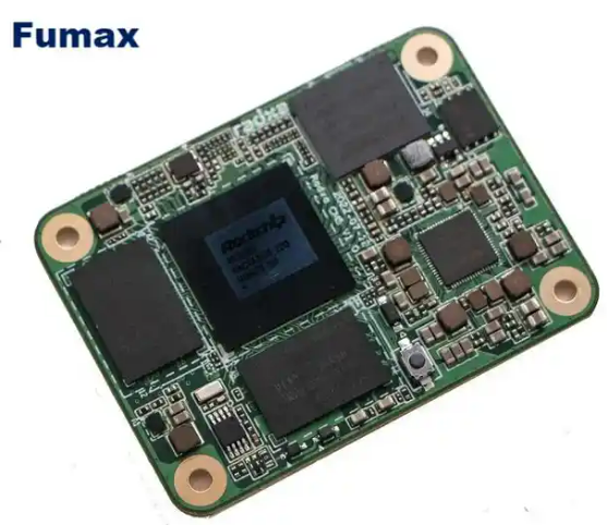
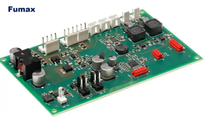
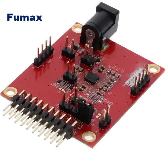
PCB cloning manufacturers in China
PCB Printed Circuit Board Cloning Manufacturers Near Me. In China, there are many PCB cloning manufacturers, such as Shenzhen Fumax Technology Co., Ltd., Shenzhen Wangshengjie Electronics Co., Ltd., Shenzhen Jingke Yulon Electronics Co., Ltd., and Shenzhen Jingxin Precision Circuit Co., Ltd.
These manufacturers have certain capabilities in PCB design, manufacturing and processing, and can provide various types of PCB boards, including circuit boards, aluminum substrates, flexible boards, PCB boards, LED aluminum substrates, LED light strip boards, pcba finished boards, etc. .
If you need more detailed information, it is recommended to contact these manufacturers by phone or email.
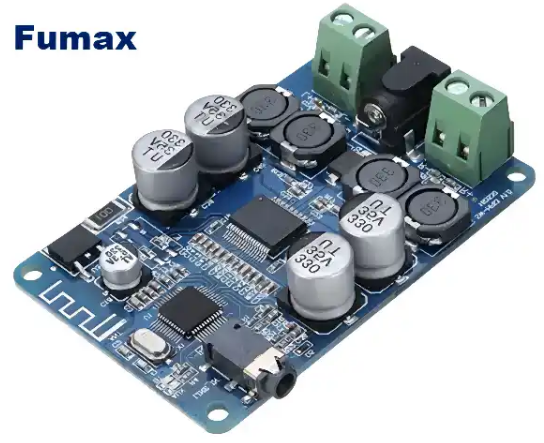
There is a well-known PCB cloning manufacturer in Shenzhen, Shenzhen Fumax Technology Co., Ltd. Our company specializes in double-sided, multi-layer PCB copy boards (clone boards), board modifications, BOM list production, reverse schematic diagrams, SMT processing, chip decryption, prototype production, PCB production/mass production (including debugging), and is A high-tech enterprise specializing in providing complete solutions for electronic products to global customers.