In the PCB design process, copper cladding is an important aspect, and various PCB design software provide intelligent copper cladding functionality, which covers unused spaces on the PCB with copper. The significance of copper cladding lies in reducing ground impedance, enhancing anti-interference capability, lowering voltage drop in power traces, improving power efficiency, and connecting to ground to minimize loop area.
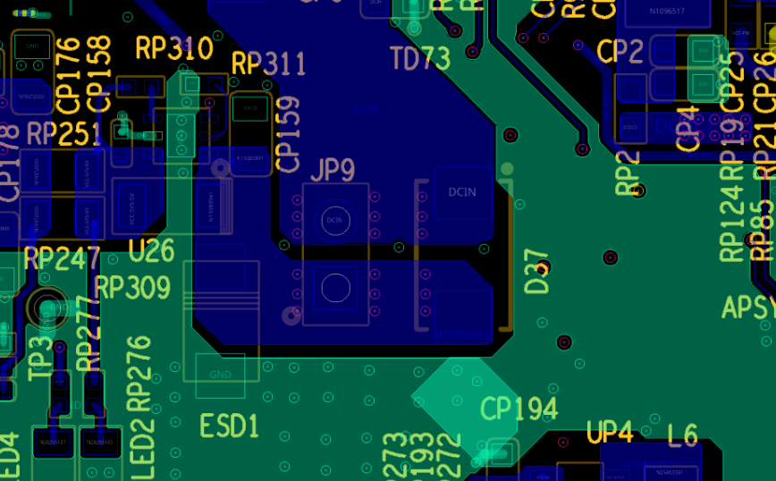
PCB copper cladding refers to the area in the PCB layer filled with copper. This layer can be on the top, bottom, or any internal layer of the PCB stack, and PCB copper cladding can be used for grounding, reference, or isolating specific components or circuits from the rest of the layer. After layout and routing are completed, there are often many vacant areas on the surface of our PCB. We use GND or some power network to cover these areas with a solid copper layer.
In digital circuits, there is a large amount of sharp pulse current, so reducing ground impedance is more necessary. It is generally believed that for circuits composed entirely of digital devices, large-area grounding should be adopted. However, for some analog circuits, the ground loop formed by copper cladding may cause electromagnetic coupling interference, which is not worth the gain.
Advantages of PCB copper plating:
- Electromagnetic Compatibility (EMC): Large areas of copper plating on ground or power can shield electromagnetic interference, enhance circuit’s anti-interference ability, and meet EMC requirements.
- PCB manufacturing requirements: Copper plating helps ensure the uniformity of electroplating, reduces deformation of the board during lamination, and improves the manufacturing quality of PCBs.
- Signal integrity: Provides a complete return path for high-frequency digital signals, reduces direct current network wiring, and enhances the stability and reliability of signal transmission.
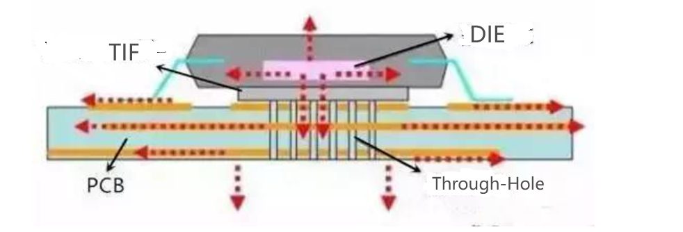
- Heat dissipation: Proper copper plating can improve the heat dissipation performance of PCBs, reduce component operating temperatures, and increase system reliability and lifespan.
Disadvantages:
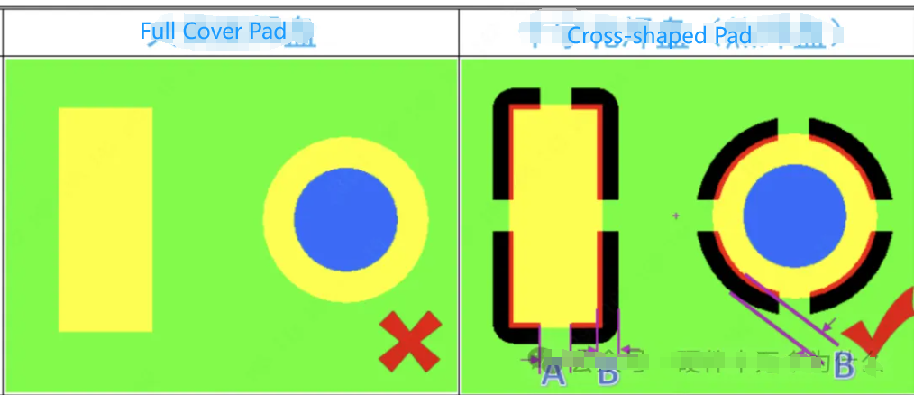
1.Rapid heat dissipation, difficult soldering: Full coverage of component pins with copper plating may lead to rapid heat dissipation, making desoldering and rework difficult. Copper has a high thermal conductivity, causing rapid heat dissipation during soldering, affecting the soldering process. Therefore, the design should minimize heat dissipation by using “cross-shaped solder pads” to facilitate soldering.
2. Signal Weakness and Interference: Copper plating around the antenna section may result in signal weakening and interference, affecting signal acquisition. The impedance of copper plating may also impact the performance of amplification circuits, hence copper plating is generally avoided in these areas.
3 Processing Complexity: Copper plating requires consideration of the impact of each plating area during the design process. Improper design may increase processing complexity, such as the need for cross connections to avoid heat dissipation issues. However, this aspect is minimal and can be disregarded as modern processes are mature, and PCB manufacturers will not increase costs due to this.
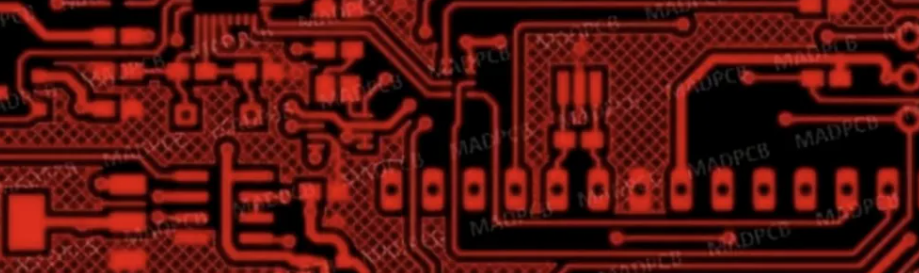
Large-area Copper Plating (Solid Copper Plating) and Grid Copper Plating:
Copper plating generally comes in two basic forms: solid copper plating and grid copper plating
- Large-area Copper Plating:
It serves a dual purpose of increasing current and shielding. However, during wave soldering, it may cause board warping or even bubbling. In such cases, it’s common to create several slots to reduce air bubbles in the copper foil.
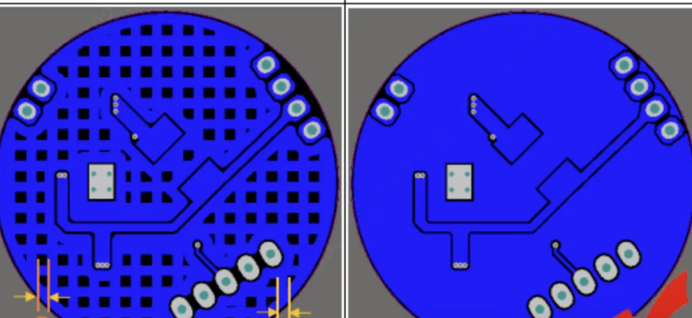
- Mesh Copper Plating:
It mainly serves as a shielding function. Because the cross-sectional area of the copper foil is reduced, its current carrying capacity is relatively weaker compared to solid copper plating.
When choosing the method of PCB copper plating, both mesh copper plating and solid copper plating have their advantages and disadvantages, depending on the design requirements and application scenarios. Here is a comparison between them:
- Mesh Copper Plating:
- The mesh structure may increase the complexity of PCB manufacturing, especially requiring more attention in design and processing. However, as long as the grid is not too small and excessive fragmented copper is not added, the impact is minimal.
- For some high-frequency and high-speed signals, mesh copper plating may increase signal transmission loss, leading to signal integrity issues. If copper plating serves as a reference plane for PCB routing, it’s better to avoid using mesh copper plating and opt for complete plane copper plating to achieve a complete reference plane.
- It can reduce the weight of the PCB, especially in large PCBs, contributing to overall weight reduction. Generally, the impact is minimal.
- It is more flexible in dealing with thermal expansion and mechanical stress, reducing the impact of PCB deformation under heat and stress.
- Compared to mesh copper plating, solid copper plating increases the weight of the PCB because it uses more copper material.
- It provides maximum conductivity and grounding connections, making it an ideal choice for applications requiring high conductivity.
- In some high-frequency and high-speed signal PCB designs, providing a complete reference plane, solid copper plating helps reduce signal transmission loss and improve signal integrity.
- In some scenarios, solid copper plating can provide better shielding effects, reducing electromagnetic interference.
Shielding Effects of Large-Area Copper Plating (Solid Copper Plating) and Mesh Copper Plating:
Both solid copper plating and mesh copper plating have certain shielding effects, but which one is better depends on specific application scenarios and design requirements.
Shielding Effect of Solid Copper Plating:
Solid copper plating provides more copper material, which can offer better shielding effects, especially for low-frequency and static electromagnetic interference.
Solid copper plating can form a complete conductive shielding layer, covering the entire area, blocking the entry and propagation of external electromagnetic waves, thus reducing interference.
Solid copper plating can better enclose and shield internal circuits, reducing the impact of electromagnetic radiation on the surrounding environment and other circuits.
Shielding Effect of Mesh Copper Plating:
Although mesh copper plating provides some shielding effects, its shielding effect may be slightly inferior to solid copper plating.
Mesh copper plating usually leaves gaps, allowing electromagnetic waves to partially penetrate or pass through, so its shielding effect on high-frequency or high-speed signals may be relatively poor.
However, while providing a certain degree of shielding effect, mesh copper plating reduces the use and weight of copper materials.
Regarding the Heat Dissipation Effect of Solid Copper Plating and Mesh Copper Plating:
Many online claims are unfounded. Firstly, we know that the main heat source on the circuit board is the integrated circuit, which can dissipate heat through the PCB. Then, the PCB connects to the solder pad, dissipating the heat from the integrated circuit. Therefore, the larger the area of the copper foil, the better the heat dissipation.
In terms of heat dissipation, solid copper plating typically outperforms mesh copper plating. Here’s a comparison between the two:
Heat Dissipation Effect of Solid Copper Plating:
Solid copper plating provides more copper material, which allows for better heat conduction, resulting in generally superior heat dissipation performance.
Solid copper plating forms a continuous heat conduction path, facilitating the even distribution of heat throughout the entire copper-plated area, effectively reducing the operating temperature of components.
Heat Dissipation Effect of Mesh Copper Plating:
While mesh copper plating can also contribute to heat dissipation to some extent, its heat dissipation effect may be slightly inferior compared to solid copper plating.
Mesh copper plating may be affected by gaps in heat dissipation, and the heat conduction path may not be as continuous as that of solid copper plating, resulting in relatively poorer heat dissipation.
Overall, if heat dissipation is a critical factor in the design and superior heat dissipation performance is required on the PCB, solid copper plating is often the better choice. However, in applications where heat dissipation requirements are not particularly strict or in cases where lightweight design is needed, mesh copper plating may also be a viable option. It can provide heat dissipation to some extent and reduce the weight of the PCB.