Hey there, tech enthusiasts! Get ready to dive deep into the fascinating world of circuit card assembly. In this comprehensive guide, we’ll take you through every meticulous step of the process, from PCB manufacturing to the final assembly of the board. So grab your coffee, settle in, and let’s explore the intricate journey of bringing electronic dreams to life!
1. PCB Manufacturing: Laying the Foundation
1.1 Cutting the Cloth: The journey begins with the raw material – the PCB blank. Each board is meticulously cut to the precise dimensions required for the final product. Using advanced machinery, our team ensures accuracy down to the micron, laying the foundation for what’s to come.
1.2 Drilling Down: Next up, we move to the drilling stage. Tiny holes, often smaller than a pinhead, are strategically placed on the board to accommodate the electronic components that will later be soldered into place. Precision is paramount here, as any deviation could result in misalignment during assembly.
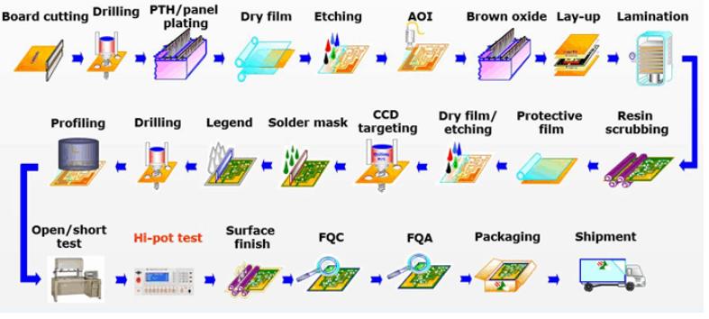
1.3 Copper Plunge: With the board prepped and holes drilled, it’s time to dive into the copper plunge. Through a series of chemical processes, a thin layer of copper is deposited onto the surface of the board, creating the conductive pathways that will form the backbone of our circuitry.
1.4 Graphic Transfer & Electroplating: Graphics come alive as they’re transferred onto the board, guiding the electroplating process that reinforces the copper pathways. This step not only enhances conductivity but also adds durability to the board, ensuring it can withstand the rigors of real-world use.
1.5 Etching Away: With the graphics in place, it’s time to etch away the excess copper. Using a precise chemical process, we remove the unwanted copper, leaving behind the intricate network of circuitry that will power our devices.
1.6 Printing Solder Mask & Silk Screen: Adding the finishing touches, solder mask is applied to protect the circuitry from environmental factors such as moisture and dust. Meanwhile, silk screen printing is used to add labels and identifiers, ensuring ease of assembly and maintenance down the line.
1.7 Pad Plating & Surface Treatment: Pads are plated to enhance conductivity and ensure reliable solder connections. Additionally, the surface of the board undergoes treatment to optimize solder adhesion, guaranteeing robust connections between components.
1.8 Shaping Up: With the board fully prepared, it’s time to shape it to perfection. Using precision cutting techniques, we trim any excess material, ensuring each board meets our exacting standards before moving on to assembly.
1.9 Testing & Validation: Before proceeding to assembly, each board undergoes rigorous testing to ensure functionality and reliability. From continuity checks to high-voltage testing, we leave no stone unturned in our quest for perfection.
2. PCB Assembly: Precision in Every Step
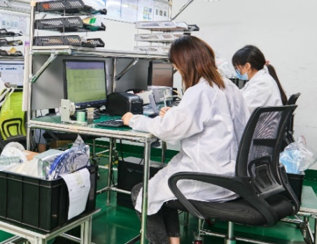
2.1 Double-Checking Files: With the boards ready for assembly, we begin by double-checking all data to ensure accuracy and alignment with customer specifications. Any discrepancies are addressed immediately to avoid issues down the line.
2.2 Tooling Up: Essential tools and equipment are prepared for the assembly process ahead. This includes fixtures for wave soldering and reflow soldering, as well as steel nets for stencil printing. Each tool is meticulously calibrated to ensure precise results every time.
2.3 Incoming Inspection: Every component that enters our facility undergoes thorough inspection to verify its quality and integrity. Components that fail to meet our standards are rejected, ensuring only the highest quality materials are used in our assembly process.
2.4 SMT Assembly: Surface Mount Technology (SMT) is the cornerstone of modern electronics assembly. This process involves several intricate steps, each executed with precision and care:
- 2.4.1 Solder Paste Printing: Solder paste is precisely deposited onto the board using a stencil. This paste serves as the adhesive that will hold the components in place during reflow soldering.
- 2.4.2 Solder Paste Inspection (SPI): Before components are placed, the solder paste is inspected to ensure proper volume and placement accuracy. Any discrepancies are corrected immediately to avoid issues during assembly.
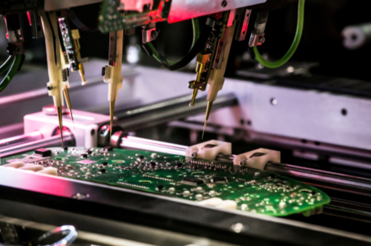
- 2.4.3 Component Placement: Advanced pick-and-place machines precisely place each component onto the board. These machines work at lightning speed, placing thousands of components per hour with incredible accuracy.
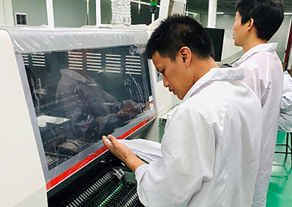
- 2.4.4 Reflow Soldering: Once all components are in place, the board enters the reflow oven. Here, it is subjected to carefully controlled temperatures that melt the solder paste, creating strong, reliable connections between the components and the board.
- 2.4.5 Automated Optical Inspection (AOI): After reflow soldering, each board undergoes comprehensive visual inspection using AOI systems. These systems use advanced cameras and algorithms to detect any defects or irregularities in component placement or solder joints.
- 2.4.6 First Article Inspection (FAI): The first assembled board from each batch undergoes additional inspection to ensure compliance with specifications and quality standards. This thorough inspection process ensures that any issues are caught and addressed early, minimizing waste and rework.
2.5 Through-Hole Assembly & Finalization:
- 2.5.1 Wave Soldering: For through-hole components, we turn to wave soldering. This process involves passing the board over a wave of molten solder, which creates strong, reliable connections between the components and the board.
- 2.5.2 Cleaning & Preparation: After soldering, the boards are thoroughly cleaned to remove any flux residue or contaminants. This ensures the final product meets our high standards for cleanliness and reliability.
- 2.5.3 Component Integration: Additional components, such as cables, connectors, and heat sinks, are carefully integrated into the assembly. Each component is placed with precision and care, ensuring optimal performance and reliability.
- 2.5.4 Enclosure Assembly (If Applicable): For products requiring enclosures, the final assembly stage involves fitting the boards into their designated enclosures. This step ensures the finished product is protected from environmental factors and meets any aesthetic requirements.
- 2.5.5 Functional Testing: Before leaving our facility, each assembled board undergoes rigorous functional testing. This testing ensures that the board performs as intended and meets all customer requirements.
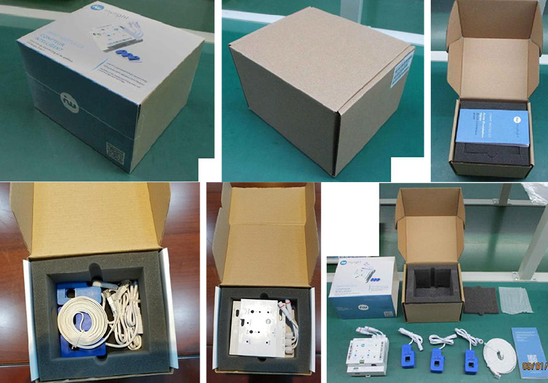
- 2.5.6 Packaging & Shipping: Finally, the boards are carefully packaged to protect them during transit and shipped to their destination. Each package is labeled with care instructions and handling guidelines to ensure the product arrives safely and intact.
And there you have it, folks! From the birth of a PCB to its final assembly, each step in the process is meticulously executed with precision and care. It’s this attention to detail that sets us apart and ensures that our products meet the highest standards of quality and reliability. So, the next time you pick up a device, take a moment to appreciate the journey it took to get into your hands. It’s a journey filled with innovation, dedication, and a relentless pursuit of perfection.