Editor’s Note: In modern high-speed designs, analyzing signal integrity, power integrity, and EMC separately is not enough; a holistic approach is essential for successful design.
Background Issue: When signals cross over segmentation areas between adjacent reference planes on a layer, discussions about signal integrity often arise. Some argue that signals should not cross the segmentation as it may increase crosstalk and EMC issues, while others suggest that with careful design of layer stackup and width of segmentation gaps on power/ground planes, there shouldn’t be a problem. So, what’s the right approach? Of course, the best answer is “it depends!” This article explores the scenario when signals pass through segmented planes.
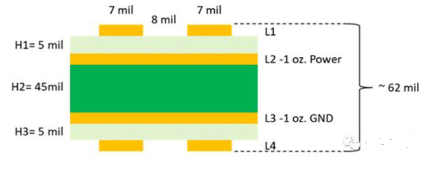
First, let’s consider a typical four-layer PCB stackup with a total thickness of 62 mils. The surface layer is the signal layer, while the inner layers are the plane layers. The trace width is 7/8 mil, with a differential impedance of 100 ohms and a single-ended impedance of 56 ohms.
In modern electronic product design, having multiple power rails in a product is quite common, which means that the power plane in a four-layer board will inevitably be divided. Therefore, the presence of signal crossings over splits is unavoidable during routing.
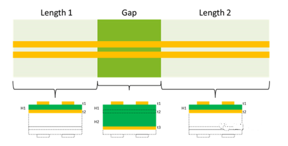
Assuming a pair of surface transmission lines crossing a 50-mil wide gap between adjacent layers, as shown in the figure, the cross-section of the microstrip line before and after passing through the gap is illustrated. The dielectric thickness H1 from the surface to the adjacent power reference layer is considered. Since there are no adjacent power reference planes at the gap, and the next reference plane is the ground adjacent to the bottom layer, the dielectric thickness at the gap is equal to H1 plus the thickness of the 1oz power layer, plus the next dielectric layer H2. If the thickness of the power layer is 1.2mil, then the total dielectric thickness at the gap is 51.2mil.
The first-order approximation of this topology is a combination of three segments of transmission lines with two different impedances. The first and last segments are both 100ohm differential impedance and 56ohm single-ended impedance, while the transmission line in the gap part has a differential impedance of 134ohm and a single-ended impedance of 103ohm. Its impedance is higher than other parts, causing signal reflection here. The height and width of the reflection are functions of the corresponding signal rise time and gap geometry. The faster the rise time, and the wider the gap, the greater the reflection caused. Figure 3 shows the simulation results.
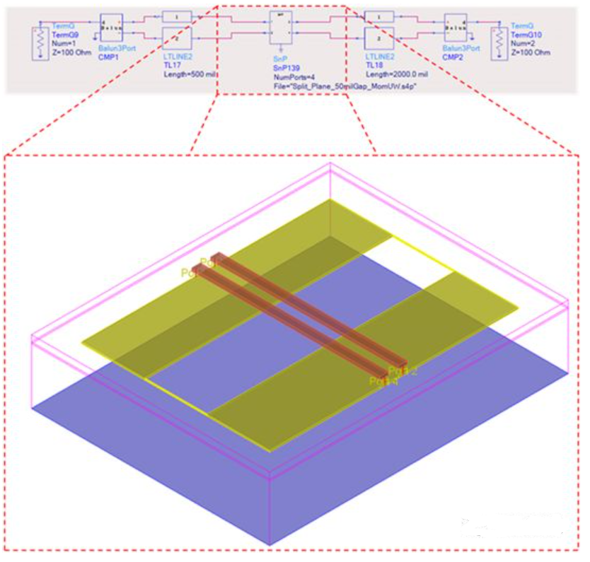
The first and third segments of transmission lines are simulated using the 2D model of TLines-LineType (ADS), while the transmission line at the gap is simulated using a 3D electromagnetic field solver (Momentum or EMPro) to obtain the electromagnetic field effects when the signal passes through. The dielectric materials are the same. S-parameters are extracted and used in the schematic.
The total length of the topology is 2.65 inches, with the length of the first segment of the transmission line (L1) being 500 mils, and the length of the third segment (L2) being 2 inches. The 3D part is divided into three segments of 50 mils each to facilitate adjustment of the gap width while ensuring the total length remains unchanged.
Two gap widths are used to compare the effects of gap size. A 50 mil gap between power planes is common and represents the worst-case scenario. A 5 mil gap is the optimal scenario and is also the typical minimum value from the transmission line to the solder pad.
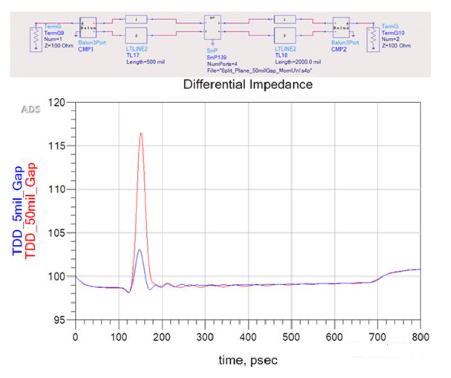
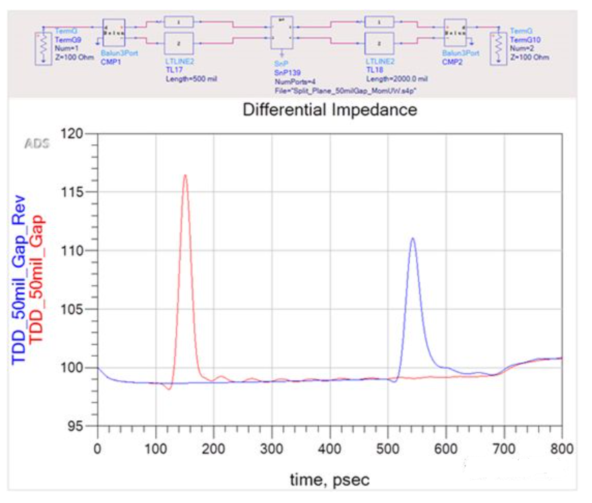
A differential excitation source is applied at port 1, and the comparison of differential impedances is shown in Figure 4. To facilitate viewing the impedance at port 2, a balun converter is used to convert port 4 to port 2. The red curve represents the results for a 50 mil gap, which exhibits higher impedance discontinuity compared to the results for a 5 mil gap (blue curve). This is because the height of the emitted pulse is determined by both the rise time and the gap width. Since the rise time is smaller in spatial length compared to the gap width, solely changing the rise time cannot achieve the maximum impedance discontinuity. This will be demonstrated through simulation below.
An excitation source is applied at port 2, with a 50 mil gap, and compared to the input signal from port 1, as shown in the following figure. Due to a delay of 2.05 inches before the gap, along with losses in the transmission line, the signal edge will be slower. As expected, the amplitude of the reflection is indeed lower.
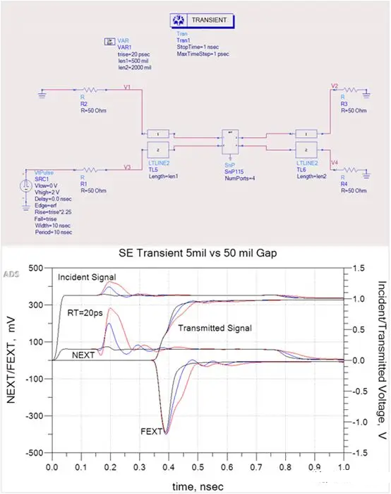
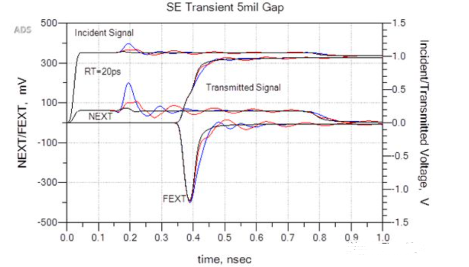
Here’s the analysis of the single-ended case, as shown in the figure. The red curve represents a 50 mil gap, the blue curve represents a 5 mil gap, and the black curve represents no gap. With a rise time of 20 ps, the reflection voltage is highest when the gap is 50 mil, resulting in a slight increase in transmission line delay compared to the case with no gap.
In all three scenarios, typical near-end crosstalk and far-end crosstalk curve variations can be observed. The tight coupling between transmission lines through the gap results in higher reflections, leading to greater near-end crosstalk.

Here’s the analysis of the single-ended case, as shown in the figure. The red curve represents a 50 mil gap, the blue curve represents a 5 mil gap, and the black curve represents no gap. With a rise time of 20 ps, the reflection voltage is highest when the gap is 50 mil, resulting in a slight increase in transmission line delay compared to the case with no gap.
In all three scenarios, typical near-end crosstalk and far-end crosstalk curve variations can be observed. When passing through the gap, the tight coupling between transmission lines results in higher reflections, leading to greater near-end crosstalk.
When there’s a 50 mil gap, near-end crosstalk pulses significantly increase, while far-end crosstalk only slightly increases. Unlike near-end crosstalk voltage, the peak value of far-end crosstalk voltage varies with coupling length. At a certain time delay (TD), its amplitude peaks at around 50% of the rise time of the attacking line signal.
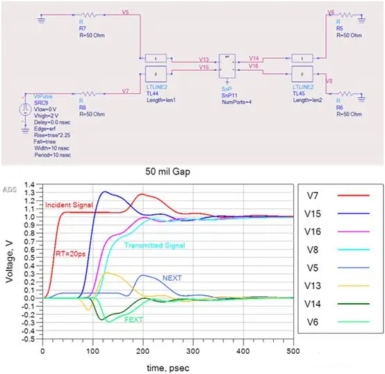
Similarly, the signal from the attacking line couples to the far-end crosstalk voltage, which couples back to the attacking line, affecting the rise time. The waveform at the far end of the attacking line is the superposition of the far-end crosstalk voltage and the original signal voltage, resulting in no crosstalk. As the far end is 2.65 inches away from the source end, far-end crosstalk is nearing saturation. Reducing the length of the last segment of the transmission line to 100 mil, as shown in Figure 7, makes it easier to understand the impact of the gap on far-end crosstalk.
The red curve represents the input signal (V7) with a rise time of 20 ps, the cyan curve (V8) represents the waveform of the transmitted signal at the far end, light blue (V5) represents near-end crosstalk, light green (V6) represents far-end crosstalk, and dark green (V15) represents the attacking signal at node V13 after passing through TL44. Due to the high impedance characteristics in the gap section, overshoot caused by increased reflections can be seen on this transmission line segment.
The orange waveform (V13) shows far-end negative crosstalk pulses, consistent with the rising edge of the attacking signal at V15. Near-end crosstalk also aligns with the positive reflection at V15. As the attacking signal experiences a delay when passing through the gap, the additional voltage swing of the reflection increases the amplitude of far-end crosstalk pulses, and its inverted shape reflects the shape of the reflected pulse, as seen in the dark green waveform (V14), which then couples back to the attacking signal and causes the rise time to decay until leaving the coupling section, as shown by the magenta curve (V16).
The problem addressed in this article is that when a signal passes through a segmented plane, the transmitted signal undergoes positive and negative reflections due to impedance mismatches, with the reflection time equal to the time it takes to pass through the gap. This increases the amplitude of the signal and the far-end crosstalk pulses, thereby slowing down the rise time of the transmitted signal in proportion to the waveform of the far-end crosstalk.
Taking into account multiple return paths at the segmented plane and edges, an effective slot antenna is formed, radiating noise outward. To meet EMI FCC Class B radiation requirements (3-meter field), the radiated noise must be less than 100 mV/m between 30-80 MHz and less than 200 mV/m between 216 MHz-1 GHz.
When microstrip lines pass through segmented planes, noise can radiate into free space due to discontinuous return paths and lack of shielding. Visualization of the return current density at the gap between adjacent reference planes can be achieved through 3D simulation software.
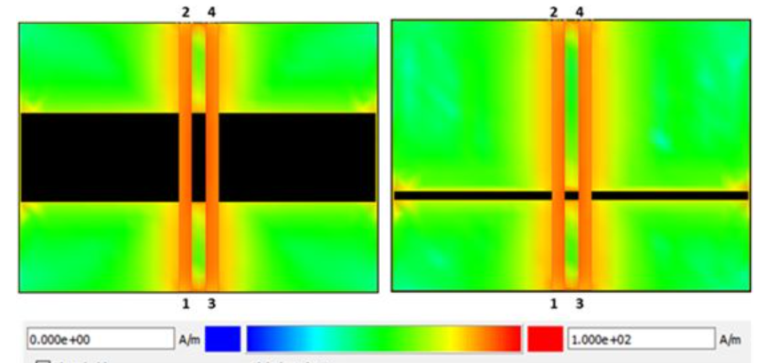
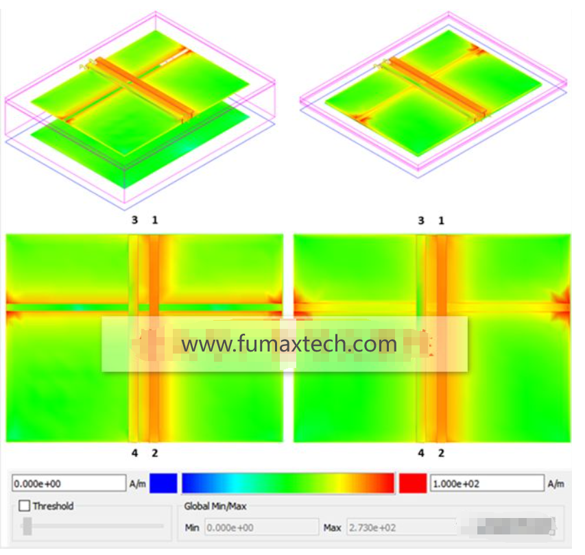
Figure 8 compares the single-ended signal return current density on adjacent reference planes. On the left, a 4 GHz sine wave passes through a 50 mil gap, while on the right, it passes through a 5 mil gap. The choice of a 4 GHz signal is because it represents the Nyquist frequency of 8 Gbps PCIe Gen 3 on a typical 4-layer PCIe board. By driving the signal from port 1 to port 2 with ports 3 and 4 properly terminated, the distribution of return current density on the reference plane at the segmentation can be clearly observed.
Note the slight increase in current density at the edges of the gap where the victim line is located. This indicates that the return current on adjacent lines causes additional far-end crosstalk voltage, as discussed earlier. From this perspective, single-ended lines crossing segmentation may not be an optimal approach.
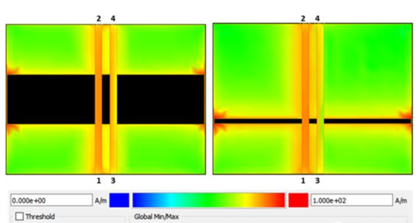
Figure 9 shows the return current density on the reference plane when a 4 GHz differential signal passes through 50 mil (left) and 5 mil (right) gaps. It can be observed that the maximum current density between the two differential pairs is concentrated at the edges of the segmentation, with only a small portion propagating along the gap.
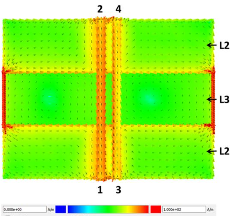
When a single-ended signal is input from port 1 to port 2, with the other ports terminated, Figure 10 displays the direction of the currents on the plane layers L2 and L3. It can be observed that when the current direction is from port 2 to port 1, the return current on L2 is split into two parts at the far end of the gap (port 1 side). Additionally, there are two reverse-rotating currents on L3, mainly concentrated on the left and right halves of the gap. These are caused by reverse-rotating currents along the edge of the gap on L2 injecting EM energy into the plane cavity. It is noteworthy that the direction of the rotating currents on L2 and L3 is opposite.
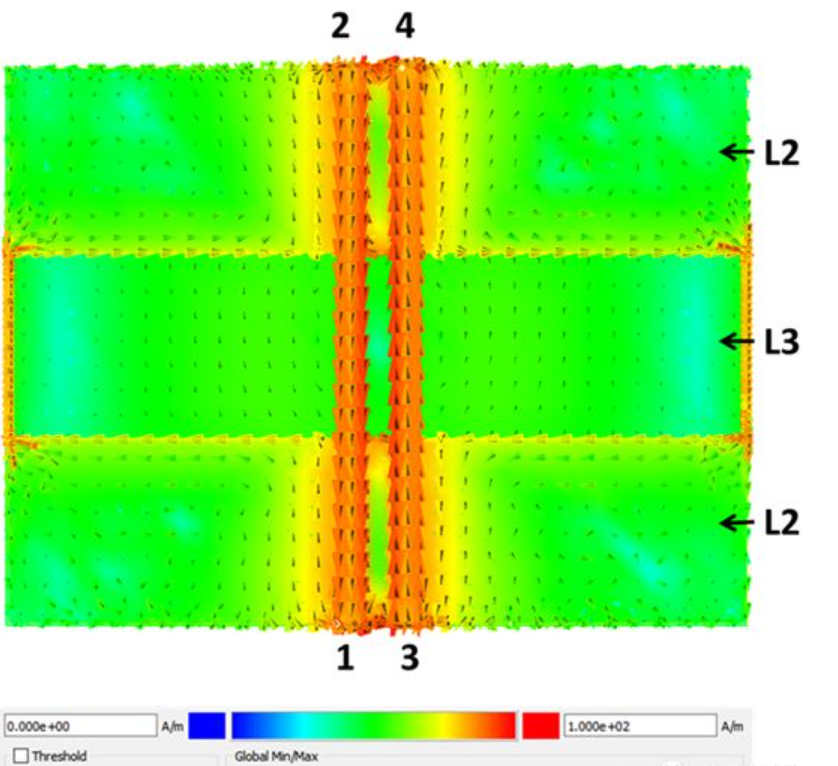
However, when a differential signal is applied to the two transmission lines, as shown in Figure 11, it can be observed that the direction of the current along the edge of the gap is the same. It is also important to note that the rotating current on L3 is unidirectional, concentrated between the differential pairs and the gap. The issue here is that even when a differential signal is applied to the two transmission lines, there is still current flowing to the edge of the gap, introducing noise into the plane cavity and radiating into free space, causing EMI.
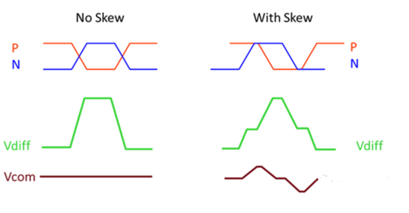
In the previous analysis, the example of a differential pair assumed perfect internal matching, but in reality, such cases are rare. Factors like unequal routing lengths, fiberglass effects, differences in connector pin lengths, or asymmetry in the differential vias when changing layers can lead to internal delay mismatches. When these situations occur, some common-mode signals can be converted into differential-mode signals. As shown in Figure 12, the degree of conversion depends on the internal delay mismatch. In an ideal differential pair, Vdiff represents the voltage difference between P and N signals. If their phase difference is 180 degrees, the common-mode voltage will double, and there will be no common-mode voltage. However, when there is a skew, the phase difference of the differential pair is not 180 degrees. Considering the skew, the differential signal will deform, resulting in a common-mode voltage (Vcom). The magnitude and shape of the common-mode voltage are proportional to the phase offset. If the phases of P and N are identical, there is no differential voltage, and all of it becomes common-mode voltage. The common-mode voltage also requires a return path, and if the path is interrupted, its return current will pass through the split plane similar to single-ended return currents.
According to some PCIe wiring specifications, the worst-case skew is 0.21UI (one UI represents the time of one bit). At PCIe Gen3 8Gbps, a 0.21UI offset corresponds to 26.3ps. The scenario passing through a 50mil gap is equivalent to an internal phase shift, as shown in Figure 13, compared with the ideal situation. As expected, the common-mode voltage passes through the partition plane, and the common-mode return current is similar to the situation with single-ended lines passing through the partition plane (Figure 8). The only difference is that there is no 100% common-mode current, so there will also be differential-mode return current.
The final issue to address is that if there is an extremely thin dielectric layer between the adjacent ground layer and the partitioned power layer, it will serve as a better return path when passing through the partitioned layer. Logically, this makes sense from the perspective of signal integrity, as the impedance of transmission lines decreases with the increase in dielectric thickness between the transmission line and the partitioned reference plane.
In the previous examples, we assumed a four-layer board with a thickness of 62 mils. This almost determines the thickness of the inner layer dielectric in the stack. To move the reference plane closer to the gap between the power planes, the PCB layer count needs to be increased to at least 6 layers to maintain stack symmetry and total thickness.
If the thickness of the dielectric below the gap is reduced, re-simulating the 5 mil gap, single-ended case, the results are shown in Figure 14. This thin dielectric layer is set to 2 mils, which is a common thickness for decoupling buried capacitance cores on the power plane. Adding the thickness of 5 mils for H1 and 1.2 mils for the power plane L2, as shown in Figure 1, the total dielectric thickness below the gap is 8.2 mils.
In the left image, most of the return current is seen being diverted around the gap in the reference plane L2. In the right image, when the signal passes through the gap, most of the return current flows towards the reference plane L3 below the transmission line, but some current still remains near the gap in L2, thereby radiating some noise.
From the perspective of signal integrity, the reflected signals and near-end crosstalk noise have been essentially halved, as shown in Figure 15. There is less attenuation in the rise time of the transmitted signal, and the far-end crosstalk has also been improved.
Returning to the main question, which perspective is correct? Neither is entirely correct. This article discusses several scenarios of microstrip lines passing through split planes. From a signal integrity perspective, under certain conditions, it may be acceptable for microstrip lines to pass through split planes. For example, in the simulation above, as long as the gap between split planes is reduced to 5mil and a thin dielectric layer is added between adjacent plane layers, crosstalk does not significantly increase. According to actual noise tolerances, this may not have an impact.
However, from an EMC perspective, there are still more risks and concerns. There is never a scenario where some returning current will never flow to the edge of the split plane gap, hence there is still a risk of EMI. Due to the multitude of interrelated factors in actual designs, it’s challenging to have a universal rule applicable here, or in any other situation.
Generally, microstrip lines should avoid crossing split planes. However, when detailed analysis of the actual layout and board stack-up is not feasible, alternative methods to mitigate noise radiation, such as adding additional external shielding, may be explored.
Ultimately, this article emphasizes that in modern high-speed designs, we cannot limit ourselves to considering only signal integrity, power integrity, or EMC individually. All three must be considered simultaneously. If we only consider signal integrity without EMC considerations, we may draw incorrect conclusions, leading to potential failure in EMC compatibility testing of the final product.