Hey there, tech enthusiasts! Get ready to dive deep into the fascinating world of circuit card assembly. In this comprehensive guide, we’ll take you through every meticulous step of the process, from PCB manufacturing to the final assembly of the board. So grab your coffee, settle in, and let’s explore the intricate journey of bringing […]
Posts in the Case study category:
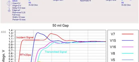
Optimizing High-Speed Design: Balancing Signal, Power, and EMC for Success
Editor’s Note: In modern high-speed designs, analyzing signal integrity, power integrity, and EMC separately is not enough; a holistic approach is essential for successful design. Background Issue: When signals cross over segmentation areas between adjacent reference planes on a layer, discussions about signal integrity often arise. Some argue that signals should not cross the segmentation […]
PCB copper cladding
In the PCB design process, copper cladding is an important aspect, and various PCB design software provide intelligent copper cladding functionality, which covers unused spaces on the PCB with copper. The significance of copper cladding lies in reducing ground impedance, enhancing anti-interference capability, lowering voltage drop in power traces, improving power efficiency, and connecting to […]
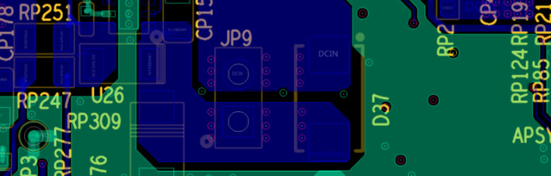
PCB Pad Design Guideline(2)
4.3.9 When designing multilayer boards, attention should be paid to components with metal casings that are in plug-in packages and make contact with the printed circuit board. The top layer pads must not be opened. They must be covered with green oil or silkscreen ink (such as two-pin crystals, three-pin LEDs). 4.3.10 When designing and […]
PCB Pad Design Guideline(1)
Standardize the PCB pad design process, define the relevant parameters of PCB pad design process, ensuring that the PCB design meets technical specification requirements such as manufacturability, testability, safety regulations, EMC, and EMI, and construct the advantages of process, technology, quality, and cost in product design. This specification applies to the PCB process design of […]
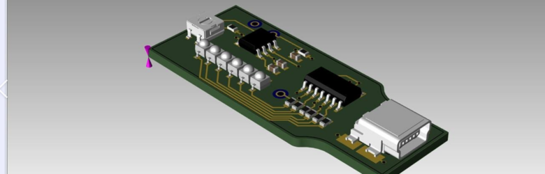
Optimizing PCB Assembly: A Seamless Customer Order Journey
In the dynamic landscape of electronics manufacturing, efficient execution of customer orders is paramount. At our state-of-the-art facility, we pride ourselves on seamlessly orchestrating the production process from inception to delivery, ensuring client satisfaction at every step. In this article, we delve into the intricate journey of a customer’s order, shedding light on how PCB […]
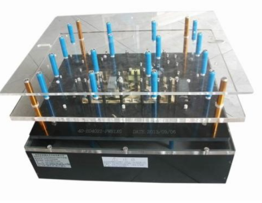
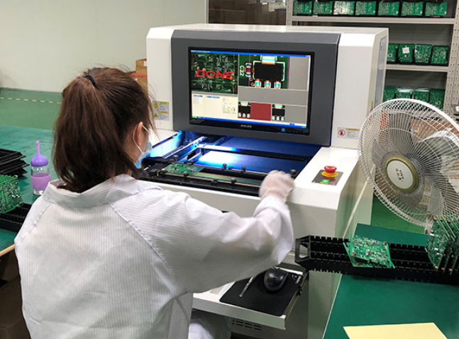
Application fields and characteristics of PCB board automatic assembly equipment
Application fields and characteristics of PCB board automatic assembly equipment PCB board automatic assembly equipment, also known as PCB board automatic assembly machine, is a device that uses automation technology to automatically assemble electronic components. It can automatically assemble surface mount components (SMD) and aperture plug-ins (THT) onto the printed circuit board (PCB), and complete […]
Understanding HDI PCB Stackup: A Comprehensive Guide
In the world of electronics and printed circuit boards (PCBs), High-Density Interconnect (HDI) technology has emerged as a game-changer. HDI PCBs offer enhanced electrical performance and compact designs, making them a popular choice for modern electronic devices. In this comprehensive guide, we’ll delve into what HDI PCB stackup is, its significance, and how it can […]
HDI PCB’s Advantages in Industrial electronics
Why HDI and how does it work In the realm of industrial control systems, High-Density Interconnect (HDI) Printed Circuit Boards (PCBs) have emerged as transformative components, revolutionizing the landscape of modern manufacturing and automation. HDI PCBs play a pivotal role in enhancing the functionality, reliability, and compactness of various industrial devices, facilitating an era of […]
Section 1: IoT PCB Assembly Expertise
Welcome to a world where IoT innovation is redefined through impeccable PCB assembly. As a leading contract manufacturing specialist, we take pride in our mastery of IoT PCBA (IoT PCB assembly). In this comprehensive guide, we will delve deep into our expertise, focusing on how we prioritize defect prevention to elevate your IoT products.
1.1. IoT Demands Unmatched Precision
IoT devices operate on the cutting edge, demanding precision in design and assembly. Our team specializes in crafting PCBs that meet the unique needs of IoT applications.
1.2. Tailored for IoT Excellence
We understand that IoT PCB assembly isn’t one-size-fits-all. Our commitment to excellence shines through in our ability to select components and create layouts that address low-power requirements and intricate IoT design challenges.
Case Study:
Section 2: Supply Chain Mastery
2.1. Crafting Components for IoT
Every IoT PCB assembly starts with component selection. Our experts are skilled at choosing IoT-centric components, ensuring that each assembly is optimized for its intended application.
2.2. Navigating the Component Maze
Component shortages can be disruptive, but our supply chain management ensures uninterrupted component flow. We proactively manage the procurement process, safeguarding your IoT projects from potential delays.
Section 3: The Defect Prevention Imperative
3.1. Quality Control at Its Zenith
Quality control is the cornerstone of our operations. We leave no room for compromise. Our rigorous quality control processes, including automated optical inspection (AOI) and in-circuit testing (ICT), guarantee that each IoT PCB is a masterpiece of reliability.
3.2. Defect Prevention: Our Core Philosophy
Defects are the antithesis of IoT reliability. We prioritize defect prevention at every step of the assembly process:
3.2.1. Reflow Soldering Artistry
Reflow soldering is the keystone of PCB assembly. Our experts control temperature profiles and solder paste deposition with precision, reducing the risk of defects like solder bridging and tombstoning to near-zero.
3.2.2. Inspection Beyond Ordinary
Our commitment to defect prevention extends to advanced inspection techniques. Automated optical inspection (AOI) leaves no solder joint or component placement uninspected. Deviations are identified, addressed, and eliminated before they become issues.
3.2.3. In-Circuit Testing (ICT) Rigor
In-circuit testing (ICT) is another layer of our defect prevention strategy. Every component and connection is probed to ensure that your IoT PCBs are free from any issues that could potentially arise during operation.
Section 4: Excellence Beyond Assembly
4.1. Beyond Assembly: A Partnership in Excellence
Our commitment doesn’t end with assembly. We believe in forging lasting partnerships that extend beyond manufacturing, working closely with you to meet your IoT product goals.
4.2. Elevating Your IoT Vision
We’re not just PCB assemblers; we’re enablers of your IoT vision. Together, we’ll elevate your IoT devices to new heights, ensuring that your innovation shines brightly in a connected world.
Conclusion
In the dynamic realm of IoT, precision and reliability are non-negotiable. Your IoT products deserve nothing less than excellence, and that’s what we deliver. At our factory, PCB assembly is not just a process; it’s an art form where defect prevention is a top priority.
Our relentless commitment to defect prevention ensures that your IoT devices are impervious to the pitfalls that can undermine performance and reliability. Partner with us, and you’re not just getting a contract manufacturer; you’re gaining a dedicated ally in your quest for IoT success.
Experience IoT PCB assembly at its zenith – reach out to us today. Together, we’ll create a future where IoT innovation knows no boundaries, and your IoT vision becomes a remarkable reality. Your IoT success story begins here!