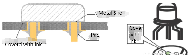
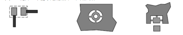
4.3.9 When designing multilayer boards, attention should be paid to components with metal casings that are in plug-in packages and make contact with the printed circuit board. The top layer pads must not be opened. They must be covered with green oil or silkscreen ink (such as two-pin crystals, three-pin LEDs).
4.3.10 When designing and laying out PCBs, try to minimize the slots and holes in the printed board to avoid affecting its strength.
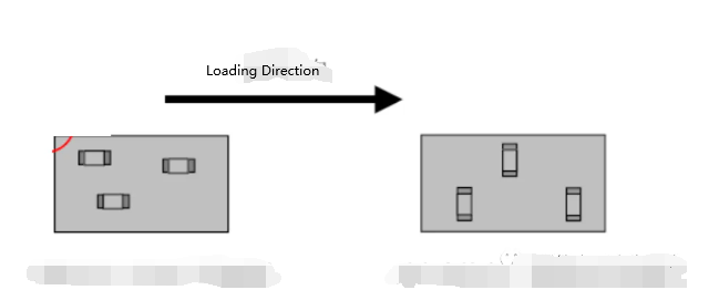
4.3.11 Valuable components: Do not place valuable components at the corners, edges, mounting holes, slots, cutting edges of panel boards, or corners. These positions are high-stress areas of the printed board, which can easily cause cracks and fractures in solder joints and components.
4.3.12 Heavy components (such as transformers) should not be far from the positioning holes to avoid affecting the strength and deformation of the printed board. When laying out, heavier components should be placed underneath the PCB (also the side that goes through wave soldering last).
4.3.13 Devices that emit energy, such as transformers and relays, should be kept away from devices and circuits susceptible to interference, such as amplifiers, microcontrollers, crystals, and reset circuits, to avoid affecting the reliability during operation.
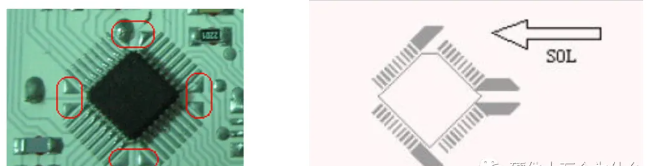
4.3.14 For ICs in QFP packages (requiring wave soldering process), they must be placed at a 45-degree angle and include solder pads (as shown in the image).
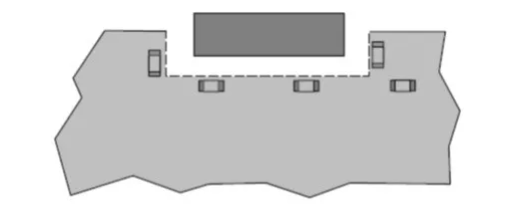
4.3.15 When surface-mount components are wave-soldered, no heat dissipation holes should be opened around and below the components with inserted components (such as heat sinks, transformers, etc.) to prevent solder from wave 1 (disturbing wave) from sticking to components or component pins on the upper board, causing foreign objects during assembly in subsequent processes.
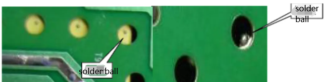
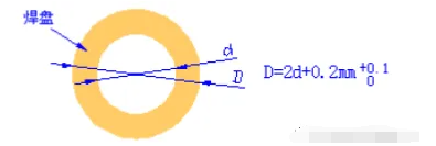
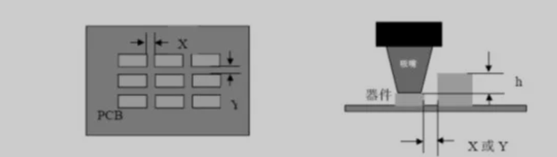
4.3.16 Large-area copper foils require insulation tape to be connected to the pads.
To ensure good solder penetration, the pads of components on large-area copper foils must be connected to the pads with insulating tape. For pads requiring more than 5A of current, insulating pads cannot be used. (See image)
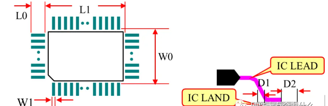
4.3.17 To avoid misalignment and tombstoning of devices after reflow soldering, the heat dissipation symmetry of the two ends of 0805 and below surface mount components should be ensured. The width of the connection between the pad and the printed conductor should not exceed 0.3mm (for asymmetric pads), as shown in the image above.
4.4 Component library selection requirements
4.4.1 The selection of existing PCB component package libraries should be confirmed to be correct.
The selection of components in existing component libraries on the PCB should ensure that the package matches the physical shape, pin spacing, hole diameter, etc., of the component.
For through-hole components, the tolerance between the component pins and the through-hole should be well-matched (the through-hole diameter is greater than 8–20mil of the pin diameter), and the tolerance can be appropriately increased to ensure good solder penetration. When no special requirements are made, the specifications of the through-hole for hand-inserted components are as follows:
4.4.2 The diameter of the components should be serialized, increasing by 5 mil for above 40 mil, namely 40 mil, 45 mil, 50 mil, 55 mil, and decreasing by 4 mil for below 40 mil, namely 36 mil, 32 mil, 28 mil, 24 mil, 20 mil, 16 mil, 12 mil, 8 mil.
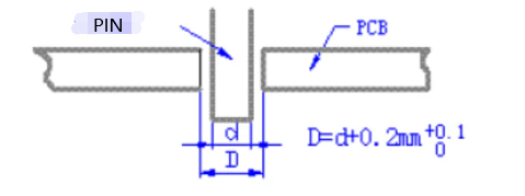
4.4.3 The correspondence between the pin diameter of the device and the pad hole diameter of the PCB, and the solder pad hole diameter of the plug pin and reflow soldering corresponds as follows:
| Device pin diameter (D) | PCB pad hole diameter/THT Reflow soldering pad hole diameter) |
| D≤1.0mm | D+0.3mm/+0.15mm |
| 1.0mm<D≤2.0mm | D+0.4mm/0.2mm |
| D>2.0mm | D+0.5mm/0.2mm |
When establishing a component package library, the unit of the hole diameter should be converted to imperial units (mil), and the hole diameter should meet the serialization requirements.
4.4.4 Design of pad shapes:
4.4.4.1 In principle, the design of component pads should comply with the following points:
4.4.4.1.1 Try to make the direction of the pad perpendicular to the direction of the flow.
4.4.4.1.2 The width of the pad is preferably equal to or slightly larger than the width of the component; the length of the pad is slightly smaller than the width of the pad.
4.4.4.1.3 Increasing the gap between component pads is beneficial for assembly; small pads are recommended.
4.4.4.1.4 There should be no through-holes on or near the pads of MT components; otherwise, during reflow soldering, the solder on the pads will flow along the through-holes, causing virtual soldering, insufficient solder, and may even flow to the other side of the board causing a short circuit.
4.4.4.1.5 The traces at both ends of the pad should be uniform or have similar thermal capacity.
4.4.4.1.6 The size of the pad must be symmetrical.
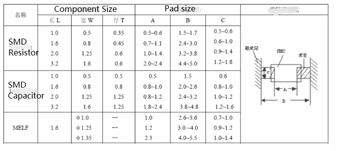
4.4.4.2 Design of solder pad shapes for chip components (see above image): The typical design dimensions for solder pads of chip components are as shown in the table below. Corresponding solder resist films can be designed outside each pad. The purpose of the solder resist film is to prevent solder bridging during soldering.
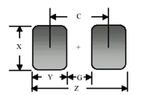
Dimensions of solder pad design for passive components – resistors, capacitors, inductors (see the table below, also refer to the above image and table)
| Part | Z(mm) | G(mm) | X(mm) | Y(ref) | |
| Chip Resistors and Capacitors | 0201 | 0.76 | 0.24 | 0.30 | 0.26 |
| 0402 | 1.45~1.5 | 0.35~0.4 | 0.55 | 0.55 | |
| C0603 | 2.32 | 0.72 | 0.8 | 1.8 | |
| R0603 | 2.4 | 0.6 | 1.0 | 0.9 | |
| L0603 | 2.32 | 0.72 | 0.8 | 0.8 | |
| C0805 | 2.85 | 0.75 | 1.4 | 1.05 | |
| R0805 | 3.1 | 0.9 | 1.6 | 1.1 | |
| L0805 | 3.25 | 0.75 | 1.5 | 1.25 | |
| 1206 | 4.4 | 1.2 | 1.8 | 1.6 | |
| 1210 | 4.4 | 1.2 | 2.7 | 1.6 | |
| 1812 | 5.8 | 2.0 | 3.4 | 1.9 | |
| 1825 | 5.8 | 2.0 | 6.8 | 1.9 | |
| 2010 | 6.2 | 2.6 | 2.7 | 1.8 | |
| 2512 | 7.4 | 3.8 | 3.2 | 1.8 | |
| 3216(Type A) | 4.8 | 0.8 | 1.2 | 2.0 | |
| Tantalum Capacitors | 3528(Type B) | 5.0 | 1.0 | 2.2 | 2.0 |
| 6032(Type C) | 7.6 | 2.4 | 2.2 | 2.6 | |
| 7343(Type D) | 9.0 | 3.8 | 2.4 | 2.6 | |
| 2012(0805) | 3.2 | 0.6 | 1.6 | 1.3 | |
| 3216(1206) | 4.4 | 1.2 | 2.0 | 1.6 | |
| 3516(1406) | 4.8 | 2.0 | 1.8 | 1.4 | |
| 5923(2309) | 7.2 | 4.2 | 2.6 | 1.5 | |
| 2012Chip(0805) | 3.0 | 1.0 | 1.0 | 1.0 | |
| Inductors | 3216 Chip(1206) | 4.2 | 1.8 | 1.6 | 1.2 |
| 4516 Chip(1806) | 5.8 | 2.6 | 1.0 | 1.6 | |
| 2825Prec(1110) | 3.8 | 1.0 | 2.4 | 1.4 | |
| 3225Prec(1210) | 4.6 | 1.0 | 2.0 | 1.8 | |
Passive Component Solder Pad Design Dimensions:
| Component | Length (mm) | Width (mm) |
|---|---|---|
| Resistor | 0.9 – 1.3 | 0.4 – 0.7 |
| Capacitor | 0.9 – 1.3 | 0.4 – 0.7 |
| Inductor | 0.9 – 1.3 | 0.4 – 0.7 |
Please refer to the above image and table for specific design dimensions and configurations.
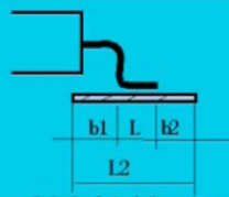
4.4.4.3 SOP, QFP Solder Pad Design: SOP, QFP solder pad sizes can be designed according to IPC-SM-782.
For the design standards of SOP, QFP solder pads (as shown in the table below):
The size of the solder pad should be determined according to the size of the component. The width of the solder pad = pin width + 2 * pin height for best soldering effects. The length of the solder pad is shown in the illustration L2, (L2 = L + b1 + b2; b1 = b2 = 0.3mm + h; h = component pin height)
4.4.4.4 When no special requirements are made, the specifications for through-hole-mounted component solder pads are as follows:
4.4.4.5 For hand-inserted PINs, capacitors, etc., with pin spacing ≤2.0mm, the specifications for solder pads are: ① Multi-layer board solder pad diameter = hole diameter + 0.2~0.4mm; ② Single-layer board solder pad diameter = 2×hole diameter

4.4.4.6 Common Surface Mount IC Solder Pad Design, see the attached file (the figure below is just a selection, see the attached file for specific dimensions)
4.4.5 New Device PCB Component Package Library Should Be Correctly Established
4.4.5.1 Devices without existing component package libraries on the PCB should establish new component package libraries based on device data, and ensure that the silkscreen inventory matches the physical objects, especially whether the newly established electromagnetic components, self-made structural components, etc., match the component library with the data (acknowledgment letter, specification sheet, drawings). New devices should establish component libraries that can meet different process requirements (reflow soldering, wave soldering, through-hole reflow soldering).
4.4.5.2 SMT components that require wave soldering should use surface mount wave soldering pad libraries.
4.4.5.3 The types of axial components and jumper pins should be minimized to reduce the molding and installation tools for components.
4.4.5.4 Different PIN spacing compatible components should have separate solder pad holes, especially the solder pads compatible with encapsulated relays should be connected.
4.4.5.5 Surface mount components should not be used as debugging components for manual soldering, as surface mount components are easily damaged by thermal shock during manual soldering.
4.4.5.6 Unless experimental verification is done without problems, surface mount components with significantly different thermal expansion coefficients from the PCB should not be selected, as this may cause solder pad delamination.
4.4.5.7 Unless experimental verification is done without problems, non-surface mount components should not be used as surface mount components. This may require manual soldering, which will result in low efficiency and reliability.
4.4.5.8 For multi-layer PCBs, local copper plating on the side as soldering pins must ensure that each layer is connected with copper foil to increase the adhesion strength of the copper plating. At the same time, experimental verification must be done without problems. Otherwise, double-sided boards cannot use side copper plating as soldering pins.
4.4.6 Safety distance for single-sided backboard components requiring wave soldering to prevent shadow effect during wave soldering, the distance between SMT components should meet the following requirements:
- Distance between the same type of components (as shown in the figure)
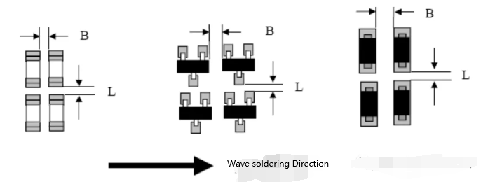
4.6.1 SMD components of the same type should have a spacing of ≥0.3mm, and the spacing between different types of components should be ≥0.13*h+0.3mm (Note: h refers to the maximum height difference between two different parts), THT component spacing should facilitate operation and replacement.
4.6.2 The distance between the outer side of the mounting component solder pad and the outer side of adjacent mounting components should be greater than 2mm.
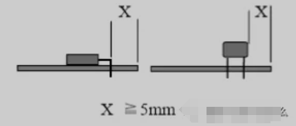
4.6.3 SMD components should be avoided within 3mm around frequently plugged components or board-edge connectors to prevent stress damage to the components during connector insertion and removal.
4.6.4 The distance from the center of the positioning hole to the edge of the surface mount component should not be less than 5.0mm.
4.6.5 Ceramic capacitors larger than 0805 packages should be placed near the transmission edge or in areas with less stress, and their axial directions should be parallel to the direction of the board’s entry, and ceramic capacitors larger than 1825 should be avoided as much as possible. (Reserved comments)
4.4.6.6 SMDs should be avoided within 3mm around frequently plugged components or board-edge connectors to prevent stress damage to the components during connector insertion and removal. See figure:
4.4.6.7 Surface-mount components for wave soldering should meet the specified requirements for stand-off. The stand-off of surface-mount components for wave soldering should be less than 0.15mm. Otherwise, they should not be placed on the B side for wave soldering. If the stand-off of the component is between 0.15mm and 0.2mm, copper foil can be placed under the component body to reduce the distance between the bottom of the component and the surface of the PCB.
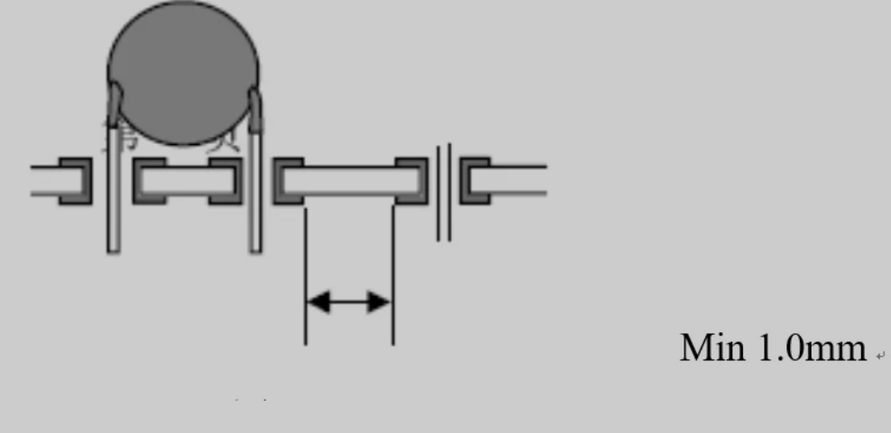
4.4.6.8 The minimum safe distance for through-hole solder points during wave soldering has been determined to ensure that solder points do not bridge during wave soldering, the distance between the edges of the back test points should be greater than 1.0mm.
4.4.6.9 The spacing between solder pads of through-hole components requiring wave soldering should be greater than 1.0mm to ensure that solder points do not bridge during wave soldering (including the spacing between the edges of component pins solder pads). The preferred pitch for through-hole component pins (pitch) is ≧2.0mm
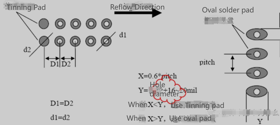
4.4.6.10 When there are many pins per row on plug-in components, and the components are arranged with solder pads parallel to the direction of PCB insertion, a recommended approach for adjacent solder pad edge spacing between 0.6-1.0mm is to use oval-shaped solder pads or to add tinning pads.
4.4.6.11 The minimum spacing between surface mount components should meet the following requirements:
For machine placement:
- Between components of the same type: ≥ 0.3mm
- Between components of different types: ≥ 0.13 * h + 0.3mm (where h is the maximum height difference between neighboring components)
For manual placement:
- Between components: ≥ 1.5mm.
4.4.6.12 The distance from the outer edge of components to the edges of the board tracks should be greater than or equal to 5mm. This is to ensure that the claws of the conveyor track do not touch the components during wave soldering or reflow soldering. If this requirement is not met, the PCB should be processed with an edge treatment, and the distance between the components and the V-CUT should be ≥ 1mm.
4.4.6.13 Adequate space should be reserved around adjustable and pluggable components for debugging and maintenance. The orientation of adjustable components and the space reserved for pluggable components should be determined based on the PCBA installation layout and the debugging method of adjustable components.
4.4.6.14 All plug-in magnetic components must have a sturdy base, and the use of plug-in inductors without a base is prohibited.
4.4.6.15 Avoid designing the pins of polarized transformers symmetrically. When a pin is not connected to a circuit, ensure that a solder pad is added to increase soldering strength.
4.4.6.16 No components or traces should be placed in the forbidden area of the mounting hole (excluding the traces and copper foil of the mounting hole itself).
4.4.6.17 The distance between metal casing components and other components should meet safety regulations. The arrangement of metal casing components should ensure that the distance from other components meets safety regulations.
4.4.6.18 Requirements for layout of components using through-hole reflow soldering: a. For PCBs with a non-conveying edge size greater than 300mm, heavy components should be avoided in the middle of the PCB to reduce the impact of the weight of inserted components on PCB deformation during soldering, as well as the impact of inserting components on components already placed on the board. b. For ease of insertion, components should be placed near the side of the insertion operation. c. For longer components (such as memory card sockets), the length direction should be consistent with the conveying direction. When multiple pins of a component are in the same straight line, connectors, DIP package components, and T220 package components should be arranged so that their axes are parallel to the direction of wave soldering. Lighter components such as diodes and 1/4W resistors should be arranged so that their axes are perpendicular to the direction of wave soldering. This prevents floating during wave soldering due to one end solidifying before the other, and avoids the use of square solder pads for through-hole components (which can lead to poor soldering and bridging).