- Purpose
Standardize the PCB pad design process, define the relevant parameters of PCB pad design process, ensuring that the PCB design meets technical specification requirements such as manufacturability, testability, safety regulations, EMC, and EMI, and construct the advantages of process, technology, quality, and cost in product design.
- Scope
This specification applies to the PCB process design of household electronic products and is applicable to activities including but not limited to PCB design, PCB batch production process review, and single board process review.
In case of any conflict between the content of this specification and the content of previous related standards or specifications, this specification shall prevail.
- References
TS—S0902010001 “Information Technology Equipment PCB Safety Design Specification”
TS—SOE0199001 “Forced Air Cooling Design Specification for Electronic Equipment”
TS—SOE0199002 “Natural Cooling Heat Design Specification for Electronic Equipment”
IEC60194 “Printed Circuit Board Design, Manufacturing, and Assembly – Terms and Definitions”
IPC—A—600F “Acceptability of Printed Board”
IEC60950
- Specification Content
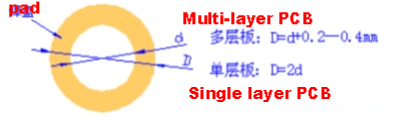
4.1 Definition of Pad The outer shape of the through-hole pad is usually circular, square, or oval. The specific size definitions are detailed below, and the noun definitions are as shown in the figure.
- Hole size:
If the physical pin is circular: Hole size (diameter) = Actual pin diameter + 0.20∽0.30mm (8.0∽12.0MIL) approximately;
If the physical pin is square or rectangular: Hole size (diameter) = Diagonal size of the actual pin + 0.10∽0.20mm (4.0∽8.0MIL) approximately.
- Pad size:
Standard pad size = Hole size (diameter) + approximately 0.50mm (20.0 MIL).
4.2 Pad Related Specifications 4.2.1 The minimum size of all single-sided pads is not less than 0.25mm, and the maximum diameter of the entire pad is not greater than three times the component hole diameter. Generally, through-hole components use circular pads, with pad diameters being at least 1.8 times the hole diameter; single-sided board pad diameters are not less than 2mm; the optimal ratio of pad size to hole diameter for double-sided boards is 2.5, and for components suitable for automatic insertion machines, the pad on the double-sided board is the standard hole diameter + 0.5—+0.6mm.
4.2.2 The distance between the edges of two pads should be preferably greater than 0.4mm, and for a row of pads perpendicular to the solder wave direction, the distance between the edges of two pads should be greater than 0.5mm (at this time, this row of pads can be regarded as a wire group or socket, and if the distance between them is too close, bridging may occur easily). In the case of dense wiring, it is recommended to use elliptical and elongated connecting pads. The diameter or minimum width of single-sided board pads is 1.6mm or ensuring a minimum of 0.3 for single-sided board single-side pad, and 0.2 for double-sided board; excessively large pads can cause unnecessary bridging. In the case of densely spaced wiring, it is recommended to use circular and elongated pads. The diameter of the pad is generally 1.4mm or even smaller.
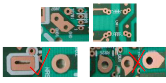
4.2.3 Pads with a hole diameter exceeding 1.2mm or a pad diameter exceeding 3.0mm should be designed as star-shaped or flower-shaped pads. For plug-in components, to avoid copper foil breakage during soldering, and the connection at the edge of the single-sided board should be completely covered with copper foil; the minimum requirement for the double-sided board should be drip-plated (see the appendix attached for details of the annular hole control section); as shown in the picture:
4.2.4 For all force-bearing devices such as socket connectors or heavy-weight devices, the width of the copper foil covering within 2mm of the pad lead should be increased as much as possible, and there should be no empty pads designed to ensure that the pads have enough tin consumption, and the copper foil will not easily peel off when the socket is subjected to external force. For large components (such as transformers, electrolytic capacitors with a diameter of more than 15.0mm, sockets with large currents, etc.), the area of enlarged copper foil and tinning on the upper side should be as shown below; the minimum area of the shaded part should be equal to the pad area. or designed as a flower-shaped or star-shaped pad.
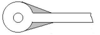
4.2.5 All machine-inserted parts should be designed as drip pads along the direction of the bent foot to ensure that the solder joints at the bent foot are full. For horizontal components, the left and right feet should be bent inward directly, and for vertical components, the left foot should be bent downward at an angle of 15°, and the right foot should be bent upward at an angle of 15°. Pay attention to ensuring that the edge spacing between them and the surrounding pads is at least greater than 0.4.

4.2.6 If there is a large-area ground and power line area on the printed circuit board (area exceeds 500mm2), it should be locally opened with windows or designed as grid filling (FILL). As shown in the picture:
4.3 Manufacturing Process Requirements for Pads
4.3.1 For surface-mounted components without connected through-hole components, test points must be added, and the diameter of the test point should be between 1.0mm~1.5mm, for easy testing with online testing equipment. The distance from the edge of the test pad to the edge of the surrounding pads should be at least 0.4mm. The diameter of the test pad should be above 1mm, and it must have a network property. The center distance between two test pads should be greater than or equal to 2.54mm; if through holes are used as measurement points, solder pads must be added outside the through holes, with a diameter of 1mm (including);
4.3.2 Pads must be added at the locations where holes with electrical connections are located; all pads must have network properties, and networks without connected components cannot have the same network name; the distance from the center of the positioning hole to the center of the test pad should be more than 3mm; other irregular shapes, but with electrical connections, such as grooves, pads, etc., should be placed uniformly in mechanical layer 1 (referring to slotted holes such as single insertion, fuse tubes, etc.).
4.3.3 For components with closely spaced pins (pin spacing less than 2.0mm), such as ICs and socket connectors, if they are not connected to hand-inserted solder pads, test pads must be added. The diameter of the test point should be between 1.2mm and 1.5mm, suitable for testing with online testing equipment.
4.3.4 If the spacing between pads is less than 0.4mm, solder mask should be applied to reduce solder bridging during wave soldering.
4.3.5 For surface-mounted components using adhesive bonding technology, solder pads should be designed at both ends and at the ends. The recommended width of the solder should be 0.5mm, and the length should generally be 2 to 3mm.
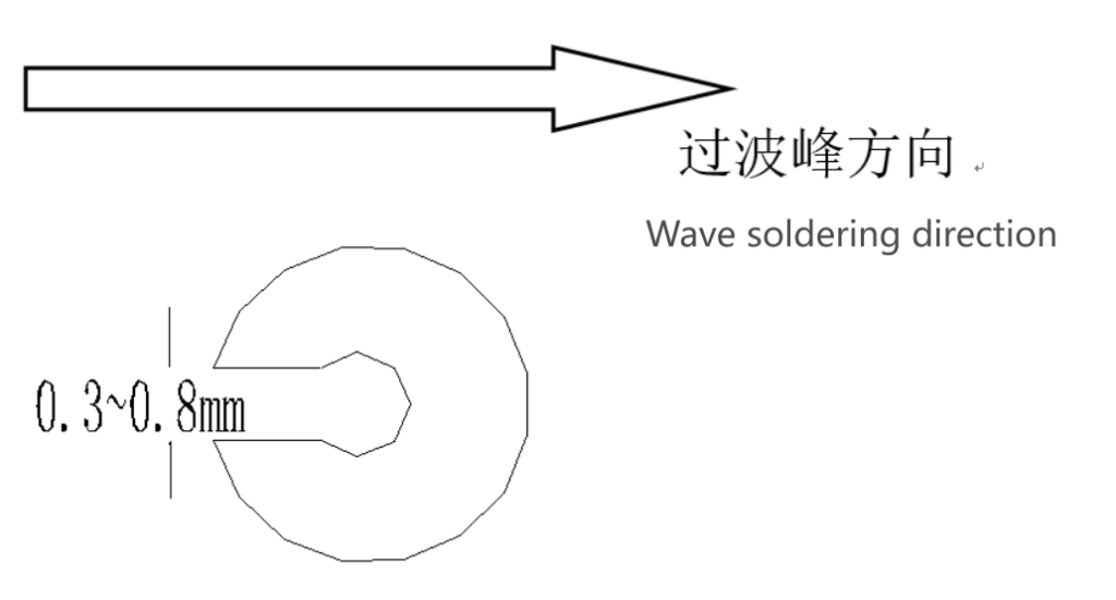
4.3.6 If there are hand-soldered components on a single-sided board, solder mask slots should be opened, with the direction opposite to the solder wave direction, and the width depends on the size of the hole, ranging from 0.3mm to 0.8mm; as shown in the figure below:
4.3.7 The spacing and size of conductive rubber buttons should match the actual size of the conductive rubber buttons. The PCB board adjacent to it should be designed as a gold finger, specifying the corresponding gold plating thickness (generally required to be greater than 0.05um~0.015um).
4.3.8 The size, dimensions, and spacing of the pads should match the dimensions of the surface-mount components.
a. When no special requirements are made, the shape of the component hole, the pad, and the shape of the component foot must match. Ensure the symmetry of the pad relative to the center of the hole (square component foot matches square component hole, square pad; circular component foot matches circular component hole, circular pad), and keep adjacent pads separate to prevent thin tin and wire drawing.
b. For adjacent component feet in the same circuit or compatible components with different PIN spacings, there should be separate pad holes. Especially for compatible relay packages, each compatible pad should be connected. If separate pad holes cannot be set due to PCB LAYOUT, the periphery of the two pads must be surrounded by solder resist.