In the world of electronics and printed circuit boards (PCBs), High-Density Interconnect (HDI) technology has emerged as a game-changer. HDI PCBs offer enhanced electrical performance and compact designs, making them a popular choice for modern electronic devices. In this comprehensive guide, we’ll delve into what HDI PCB stackup is, its significance, and how it can benefit your electronic projects.
What’s HDI PCB Stackup?
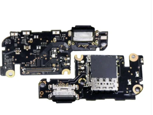
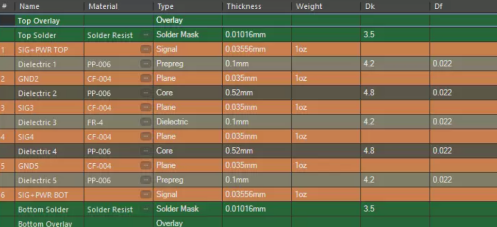
HDI PCB stackup, short for High-Density Interconnect PCB stackup, refers to the arrangement and configuration of layers in a printed circuit board using HDI technology. HDI technology involves the use of advanced manufacturing techniques to achieve a higher wiring density and miniaturization of electronic components on the board. It’s all about packing more functionality into a smaller footprint.
The Significance of HDI PCB Stackup
1. Miniaturization and Space Efficiency:
The special stackup allows for a higher component density in a smaller area, ideal for devices where space is a premium. This is particularly crucial for smartphones, wearables, and other compact electronic gadgets.
2. Enhanced Electrical Performance:
The shortened trace lengths and reduced electromagnetic interference (EMI) make HDI PCBs highly efficient in terms of electrical performance. This results in improved signal integrity and reduced power consumption.
3. Improved Signal Integrity:
With reduced noise and interference, HDI PCBs ensure that signals maintain their integrity throughout the board, leading to better performance and reliability of the electronic device.
4. Multilayer Flexibility:
HDI PCB stackup allows for multiple layers, which is advantageous when you need a high number of connections and complexity within a confined space.
5. Cost-Efficiency:
While HDI may seem intricate, they can actually be cost-effective due to the reduction in board size and the ability to utilize smaller components.
Types of HDI PCB Stackup
1. 1+N+1 HDI Stackup:
In this stackup, a single layer of high-density interconnect is sandwiched between two standard PCB layers. It’s a cost-effective option suitable for applications with medium-density interconnect needs.
2. 2+N+2 HDI Stackup:
This stackup has two layers of high-density interconnect between three standard PCB layers. It offers higher component density and is ideal for applications requiring increased routing density.
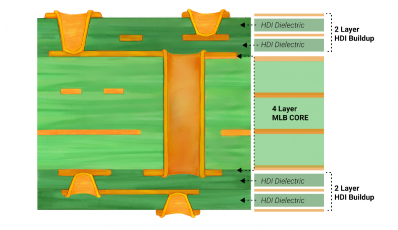
3. i+N+i HDI Stackup:
The ‘i’ in this stackup represents the number of build-up layers of high-density interconnect. It’s the most complex and offers the highest component density, making it suitable for high-end electronic devices.
Conclusion
Understanding HDI PCB stackup is essential for anyone involved in PCB design or electronics manufacturing. Its ability to enhance miniaturization, improve electrical performance, maintain signal integrity, and offer cost-efficiency makes it a preferred choice for modern electronic devices. Depending on the specific project requirements, choosing the appropriate HDI PCB stackup is crucial to ensure optimal functionality and performance of the end product. Embrace HDI technology and unlock the potential to create smaller, smarter, and more efficient electronic devices.