Demystifying High-Density Interconnect (HDI) PCBs: Production, Pitfalls, and Perfection
Hey there tech enthusiasts and fellow engineers! Ready to delve into the world of high-density interconnect (HDI) printed circuit boards (PCBs)? HDI PCBs are the backbone of today’s compact and intricate electronic devices, powering the digital era we live in. In this article, we’ll take a deep dive into how HDI PCBs are manufactured, the pesky defects that can occur during component assembly, and some pro-tips to dodge these issues right from the design phase. Buckle up, let’s unravel the magic behind HDI PCBs!
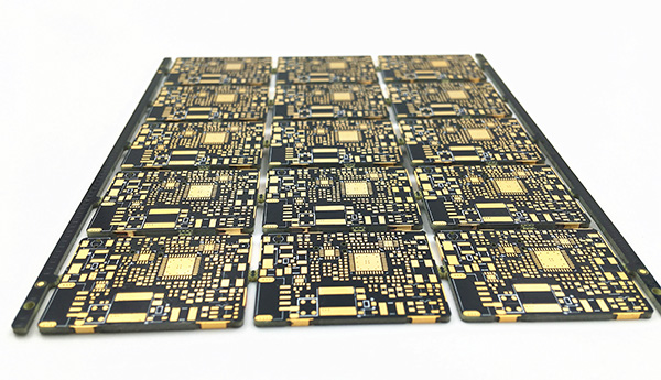
The Birth of HDI PCBs: A Glimpse into Production
HDI PCBs are like the intricate neural networks of our electronic devices, enabling them to function seamlessly. The manufacturing of HDI PCBs is a fascinating process, akin to crafting a finely detailed masterpiece. It typically involves several key steps:
1. Design and Planning:
The process commences with meticulous design and planning, envisioning the intricate circuitry and ensuring optimal space utilization.
2. Substrate Preparation:
A substrate material (often a thin core) is chosen and prepped, acting as the foundation for the PCB.
3. Lamination:
Multiple layers of copper foil and substrate are laminated together, creating the PCB’s layered structure.
4. Drilling:
Precision drilling is performed to create micro vias that establish connections between layers.
5. Copper Plating:
Copper is plated inside the drilled holes, forming the conductive pathways.
6. Imaging and Etching:
A photoresist is applied and exposed to UV light, defining the circuit patterns. The excess copper is then etched away.
7. Solder Mask Application:
A solder mask is applied to protect the copper traces and facilitate soldering during assembly.
8. Surface Finish:
The surface finish is applied to ensure solderability and durability.
9. Testing:
Rigorous testing is carried out to ensure the PCB meets quality and functionality standards.
Once this journey is complete, we have a high-density interconnect PCB ready to bring electronic dreams to life!
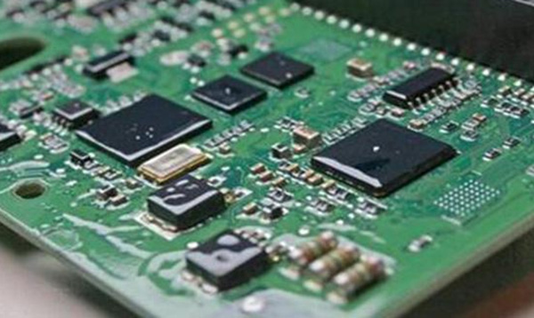
Taming the Component Assembly Beast: Common Defects and How to Avoid Them
Now, let’s shed some light on the crucial component assembly phase. While assembling the components onto the HDI PCB, a few hiccups might occur. Let’s take a look at some common defects and how we can dodge them during the design phase:
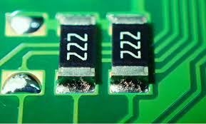
1. Solder Bridging:
This annoying defect happens when solder unintentionally connects two adjacent pads or pins. To dodge it, during design, ensure proper pad and trace spacing, considering the soldering process limitations.
2. Insufficient Solder:
When there’s not enough solder on a pad, it can lead to poor connectivity. In the design phase, ensure that the pads are appropriately sized for the components being used, avoiding excessive or insufficient solder.
3. Solder Balling:
These tiny balls of solder can form during the reflow process and cause short circuits. A well-designed solder paste stencil and optimized reflow profiles can help mitigate this issue.
4. Tombstoning:
Tombstoning occurs when a component stands vertically on one end during reflow. Proper pad design and considerations for component size and weight in the design phase can prevent this anomaly.

5. Component Misalignment:
Sometimes components may not align correctly during assembly, impacting functionality. Designing precise footprints and using appropriate pick-and-place machines can help minimize this.
Preemptive Strikes: Designing for Success
To ace the assembly phase and dodge these pesky defects, proactive measures during the design phase are key. Here are some tips:
- Collaborative Design Reviews: Involve your assembly team in the design review process. Their practical insights can be invaluable in spotting and resolving potential issues early on.
- DFM (Design for Manufacturability): Design with manufacturing in mind. Understand the capabilities and limitations of the assembly process and design the PCB accordingly.
- Clear Design Guidelines: Establish clear guidelines for trace width, pad size, and other crucial parameters to ensure a smooth assembly process.
- Regular Prototyping and Testing: Prototype and test your designs iteratively. Learn from each iteration to refine your design rules and minimize defects.
- Utilize Advanced CAD Tools: Leverage advanced CAD tools that offer features to optimize pad and trace designs, aiding in defect reduction.
Wrapping It Up: HDI PCBs – The Heart of Innovation
High-density interconnect (HDI) PCBs have indeed revolutionized the electronics landscape. They’ve empowered us to create compact, efficient, and powerful devices, driving the tech evolution. Understanding the production process and being proactive in design is crucial for producing flawless HDI PCBs and ensuring seamless assembly. So, gear up, embrace the intricacies, and let’s keep pushing the boundaries of innovation with HDI PCBs at the core.
For any inquiries or to kickstart your HDI PCB project, feel free to reach out. Happy innovating!