Multi-function MCU controlled PCB design and assembly refers to the use of MCU for circuit control and signal processing based on specific application requirements, and through PCB design and assembly technology to achieve circuit reliability and stability.
Multifunction MCU Control PCB Design and Assembly Guide
- MCU selection
First, you need to choose an MCU that is suitable for your application. When choosing an MCU, you need to consider the following factors:
- Performance: Choose an MCU with sufficient processing power and memory based on your application needs.
- Packaging: Choose the appropriate packaging type based on your PCB design and assembly needs.
- Cost: On the premise of meeting performance and packaging requirements, choose a reasonably priced MCU.
- PCB design
- Component layout: Lay out the MCU and other necessary components on the PCB, such as power supplies, resistors, capacitors, etc.
- Trace design: Design the traces on the PCB to ensure the stability and reliability of signal transmission.
- Grounding design: Design a reasonable grounding system to improve the anti-interference performance of the circuit.
- Thermal design: Consider the heat dissipation of the MCU and other components to ensure that the temperature of the PCB is stable during operation.
- Assembly Guide
- Prepare materials: Prepare required components, PCB, welding tools, etc.
- Solder components: Solder the components to the PCB according to the requirements of the schematic diagram.
- Check the welding quality: Check whether the welding point is firm and whether there is a short circuit or open circuit.
- Test function: After ensuring the welding quality, test the function of the MCU to ensure its normal operation.
- Precautions
- In PCB design, certain rules and standards must be followed, such as reasonable component layout, clear wiring, and good grounding.
- When welding components, pay attention to the welding temperature and time to avoid damage to the components and PCB.
- When testing functions, pay attention to the working status of the MCU to ensure its normal operation.
In short, multi-function MCU control PCB design and assembly need to follow certain rules and standards, while paying attention to details and skills to ensure the success of design and assembly.
Details and tips on MCU control PCB design and assembly
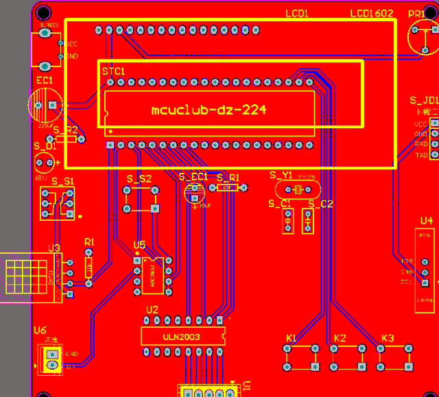
- Component layout: In terms of component layout, related components should be placed as close as possible. For example, clock generators, crystal oscillators, and the clock input terminals of the CPU are all prone to noise, so they should be placed closer together. For those devices that are prone to noise, small current circuits, large current circuit switching circuits, etc., they should be kept as far away from the logic control circuit and storage circuit (ROM, RAM) of the microcontroller as possible. If possible, these circuits can be made into separate circuits. board, which is beneficial to anti-interference and improves the reliability of circuit operation.
- Cabling design: In terms of cabling design, you need to pay attention to the following points:
a. Avoid too long traces: Excessively long traces may cause delay and interference in signal transmission.
b. Avoid traces that are too narrow: traces that are too narrow may cause signal attenuation or short circuits.
c. Avoid 90-degree angle routing: 90-degree angle routing may cause signal reflection and interference.
d. Use 45-degree angle routing: 45-degree angle routing can reduce signal reflection and interference.
e. Use shielded wires: For important signal lines, shielded wires can be used to improve the anti-interference performance of the signal.
- Grounding design: In terms of grounding design, you need to pay attention to the following points:
a. Reasonably choose the grounding method: According to the application requirements, choose single-point grounding, multi-point grounding or hybrid grounding.
b. Make sure the ground wire is thick and short: The ground wire should be as thick and short as possible to reduce the impact of the ground wire impedance on the circuit.
c. Avoid ground wire return: The ground wire should avoid forming a loop to avoid the impact of ground wire return on the circuit.
- Thermal design: In terms of thermal design, the following points need to be noted:
a. Choose the appropriate heat dissipation method: According to the heating conditions of the MCU and other components, choose the appropriate heat dissipation method, such as natural heat dissipation, air cooling or liquid cooling, etc.
b. Reasonable layout of heating components: The heating components should be as close as possible to the radiator or heat dissipation channel to reduce thermal resistance and heat dissipation difficulty.
c. Avoid overlapping components: Heating components should be placed overlapping as much as possible to reduce thermal resistance and heat dissipation difficulty.
- Component selection: When selecting components, you need to pay attention to the following points:
a. Select the appropriate package type: According to the PCB design and assembly requirements, select the appropriate package type, such as DIP, SMD or BGA, etc.
b. Select the appropriate component brand and quality level: Select the appropriate component brand and quality level based on application needs and budget to ensure component performance and quality reliability.
- Welding quality inspection: After welding is completed, quality inspection is required to ensure that there are no weak welds, short circuits or open circuits at the welding points. This can be checked using tools such as a multimeter.
- Functional testing: After ensuring the welding quality, functional testing is required to ensure that the MCU and other components are working properly. You can use oscilloscopes, logic analyzers and other tools for testing.
- PCB board cleaning and maintenance: During use, the PCB board needs to be cleaned and maintained regularly to avoid dust, dirt, etc. from affecting the circuit. You can use alcohol, cotton swabs and other tools for cleaning.
In short, MCU control PCB design and assembly requires comprehensive consideration of multiple aspects, including component layout, wiring design, grounding design, thermal design, component selection, welding quality inspection, functional testing, and PCB board cleaning and maintenance. Only by following certain rules and standards and paying attention to details and skills can we ensure the success of design and assembly and improve the reliability and stability of the circuit.
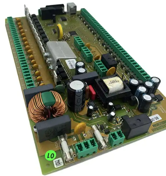
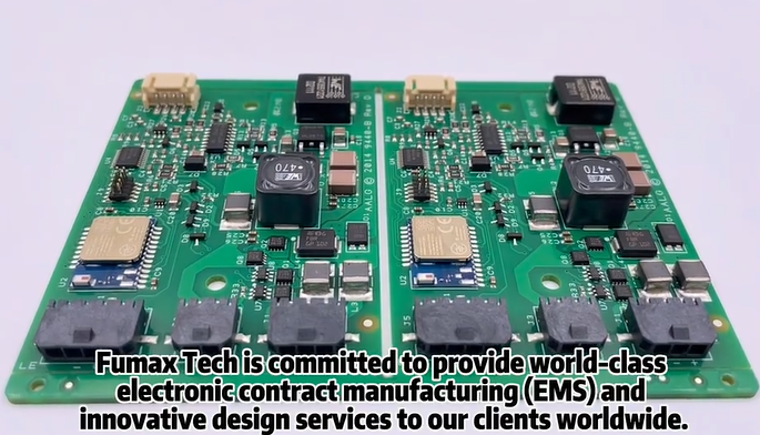
Versatile MCU controls PCB design and assembly factory
Fumax is a PCB manufacturing, assembly, and personalized customization service manufacturer.
Fumax is a company specializing in the development and design of MCU software and hardware solutions, PCBA production, and SMT processing. It has rich experience in the development of MCU application solutions and the sales of integrated circuits and intelligent control boards.
Its main service projects cover various electronic product fields such as home appliance controllers, personal care, security instruments, industrial controls, LED intelligent lighting products, intelligent hardware products, and electronic health care.
The company integrates R&D, production and sales, with a strong R&D team, professional automated production lines, and a complete after-sales service system.
To learn more about MCU control module PCB design and assembly service companies, please follow us. If you have electronic manufacturing, circuit design, and printed circuit board assembly design services, please contact us.