The Mainboard PCB assembly of the Internet of Things control system is a key link to ensure the stable and efficient operation of IoT equipment.
- Overview of the Internet of Things PCB assembly
- IoT control system motherboard PCB design
- IoT control system motherboard PCB assembly material preparation
- IoT control system motherboard PCB processing
- IoT control system motherboard PCB component welding
- IoT control system motherboard PCB assembly quality detection
- Shenzhen Fumax Technology Co., Ltd.
It involves multiple complex procedures such as the design, material selection, processing and production of PCB board. This process requires rigorous quality control and fine process management to ensure the reliability and performance of the final product.
Overview of the Internet of Things PCB assembly
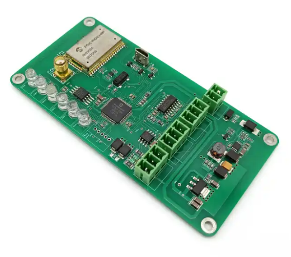
With the rapid development of IoT technology, the application of IoT devices in various fields is becoming more and more widely used. As an important part of IoT devices, the PCB assembly of the motherboard of the Internet of Things control system is a key link to achieve its high performance.
This article will detailed the entire process of the main board of the Internet of Things control system, including design, material preparation, PCB processing, component welding, quality testing and other stages, in order to provide useful references for engineers and technicians in related fields.
IoT control system motherboard PCB design
In the PCB assembly of the motherboard of the Internet of Things control system, the PCB design is the crucial first step. The factors that need to be considered in the design process include:
- Component layout: According to the circuit function and signal flow, arrange the position of the component reasonably to improve the electrical performance of the PCB board and reduce the difficulty of production.
- Selection of layers: Determine the number of layers of the PCB board according to the complexity and signal frequency of the circuit. Generally speaking, multi -layer boards can provide better electrical performance and smaller signal delays.
- Wiring planning: According to the circuit requirements, design a reasonable route and width to reduce signal loss and noise interference.
- Interface design: Consider interface requirements with other modules or devices, design appropriate connection methods and interface specifications.
- Hot design: For components with large power consumption, consider heat dissipation problems and reasonably arrange heat pipes or heat sinks.
IoT control system motherboard PCB assembly material preparation
After the design is completed, material preparation is required. This stage includes:
- Determine the list of components: List the components and its specification models required according to design needs.
- Procurement component: According to the list of components, order the required components required to the supplier.
- Detecting components: After receiving the component, quality detection should be performed to ensure that it meets the design requirements.
- Preparation: Place the qualified components in the corresponding position of the PCB board according to the process requirements.
IoT control system motherboard PCB processing
PCB processing is the process of converting the designed PCB diagram to actual PCB board, including:
- Make light -painted files: convert the designed PCB diagram into light -painted files as the basis for making boards.
- Foreign Association Manager: Give the light -painted files to a professional PCB board manufacturer for production.
- PCB board inspection: After receiving the PCB board, the appearance and size test should be performed to ensure that it meets the design requirements.
- PCB board processing: Pre -processing of necessary cleaning, drilling, etc., prepare for subsequent assembly.
IoT control system motherboard PCB component welding
After preparing the PCB board and components, welding work can be performed, including:
- Welding equipment selection: According to the need, select the appropriate welding equipment and tools, such as welding tables, welded guns, etc.
- Welding process determination: According to the types and specifications of components, formulate suitable welding process parameters, such as welding temperature, time, solder, etc.
- Equipment welding: Welded the components on the PCB board according to the process requirements.
- Welding quality inspection: After the welding is completed, perform quality inspections to ensure that welding defects without deficiency welding and short circuit.
IoT control system motherboard PCB assembly quality detection
Quality testing is an important part of ensuring product quality, including the following:
- Function test: Through various functions of the test circuit, verify whether the circuit works normally.
- Performance test: Detect the key performance indicators of the circuit, such as whether power consumption and noise meet the design requirements.
- Reliability test: Simulate the actual use environment, conduct long -term work or vibration tests on the circuit to evaluate its reliability.
- Appearance test: Check the appearance of the circuit board without obvious defects, such as scratches, stains, etc.
- Environmental adaptability test: According to the need, conduct environmental adaptability tests such as high and low temperature, humidity, to verify the performance of the circuit in different environments.
- Electromagnetic compatibility test: detect whether the electromagnetic radiation of the circuit is within the specified limit to ensure that the electromagnetic compatibility of the circuit meets the relevant standards.
Shenzhen Fumax Technology Co., Ltd.
Fumax is a professional manufacturer assembled by the main board of the Internet of Things control system. It has advanced production equipment and perfect process.
In the PCB design, material selection, processing, production and assembly, the company adheres to high standard quality control and fine process management to ensure the high reliability and high performance of the product. With excellent quality and services, the company has won widespread recognition of the industry and customers.