HDI engineers reveal the secret: Accurately master HDI PCB board blind hole detection technology to ensure the high quality and reliability of electronic products.
- HDI PCB board overview
- The Importance of HDI PCB Blind Hole Inspection
- HDI PCB blind hole detection methods and technologies
- HDI PCB board blind hole detection practical application and case analysis
- Future prospects and research directions
- HDI PCB board blind hole inspection conclusion
- HDI PCB Companies in China
HDI PCB board overview
With the rapid development of technology, high-density interconnect (HDI) PCB boards have become a key component in electronic equipment, especially in mobile devices, aerospace, medical electronics and other fields. The HDI PCB board adopts the characteristics of small holes, thin layers, and high-density wiring, making it smaller in size, lighter in weight, and higher in reliability.
As an important technology in HDI PCB board manufacturing, blind hole technology is of great significance for improving wiring density and reducing costs. Therefore, the detection of blind holes in HDI PCB boards is particularly important.
The Importance of HDI PCB Blind Hole Inspection
Blind holes are special via holes in HDI PCB boards. Due to their small diameter and no through holes at the bottom of the hole, it makes detection more difficult. However, the presence of blind vias may lead to circuit continuity issues, signal integrity issues, and PCB board mechanical strength issues. Therefore, accurate blind hole detection is an important part of ensuring the quality of HDI PCB boards.
HDI PCB blind hole detection methods and technologies
- Optical detection method: Use optical principles to observe the surface and internal structure of the PCB board through reflection and refraction. Common optical inspection equipment includes microscopes, endoscopes and AOI (automated optical inspection) equipment. These devices can detect PCB board surface defects, via holes and blind holes. The advantage of the optical inspection method is that it is non-contact and fast, but it is difficult to detect defects inside blind holes.
- X-ray detection method: Use the ability of X-rays to penetrate materials to detect the internal structure of the PCB board. For blind hole inspection, X-ray inspection method has unique advantages and can clearly display the location, shape and size of blind holes. The advantages of the X-ray inspection method are strong penetration and sensitivity to internal defects in blind holes, but the equipment cost is high and professional operators are required.
- Electrical performance detection method: determine the connectivity of through holes and blind holes by measuring the electrical characteristics of the circuit. Common electrical performance testing methods include flying probe testing and bed-of-nails testing. The advantage of the electrical performance testing method is that it is fast and highly automated, but it requires customized testing for different PCB board designs and wiring.
HDI PCB board blind hole detection practical application and case analysis
In the manufacturing process of a certain high-end smartphone PCB board, optical detection method was used to initially screen out samples with blind hole problems.
After further analysis, X-ray inspection was used to determine the location and shape of the blind holes, and it was found that some of the blind holes had incomplete internal filling.
In response to these problems, the production department has carried out process optimization and technical improvements to improve the quality and reliability of HDI PCB boards.
Future prospects and research directions
With the continuous development of technology, the manufacturing of HDI PCB boards will be more complex and sophisticated in the future. For blind hole inspection technology, it is necessary to conduct in-depth research on new optical, electrical properties and X-ray inspection methods to improve the accuracy and efficiency of inspection. In addition, intelligent and automation technology will also become a focus of future research. By introducing artificial intelligence and machine learning technology, intelligent monitoring and automatic detection of the HDI PCB board manufacturing process will be achieved, further improving product quality and production reliability.
HDI PCB board blind hole inspection conclusion
As a key component in modern electronic equipment, HDI PCB board’s quality and reliability have an important impact on the performance of the entire equipment. As an important link in HDI PCB board manufacturing, blind hole inspection is of great significance to ensure product quality and reliability.
In practical applications, it is necessary to select appropriate blind hole detection methods and equipment according to specific conditions, and continuously carry out process optimization and technical improvements to meet the evolving market demand. At the same time, it is necessary to strengthen the research and development and application of intelligent and automated technologies to improve production efficiency and product quality.
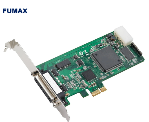
HDI PCB Companies in China
Fumax HDI PCB Company focuses on the R&D and manufacturing of high-density interconnect (HDI) PCB boards. With advanced production technology and strict quality control.
We provide customers with high-quality, high-reliability products that are widely used in communications, medical, aerospace and other fields. The company focuses on technological innovation, constantly launches new products that meet market needs, and is committed to becoming a leader in the global HDI PCB industry.