With the rapid development of IoT technology, the applications of IoT communication devices are becoming more and more widespread.
- Internet of Things communication equipment PCB circuit board design process
- Key technologies for PCB circuit boards of Internet of Things communication equipment
- Case study on PCB circuit board design of Internet of Things communication equipment
- IoT communication equipment PCB circuit board OEM design conclusion
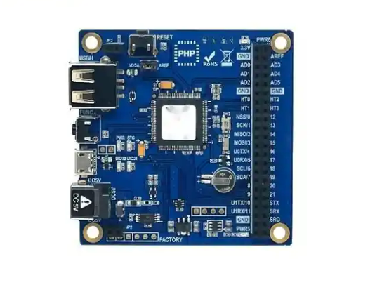
As the core component of communication equipment, PCB circuit board’s design quality and reliability play a vital role in the performance of the entire equipment.
OEM design refers to a standardized design provided by the original equipment manufacturer to meet specific customer needs. This article will provide a detailed introduction to the PCB circuit board OEM design of IoT communication equipment.
Internet of Things communication equipment PCB circuit board design process
- Demand analysis: Before starting the design, it is necessary to conduct an in-depth analysis of the customer’s needs and clarify key factors such as design goals, performance requirements, and size restrictions.
- Schematic design: Based on the requirements analysis results, design the circuit schematic and determine the connection relationship and signal flow of each component.
- PCB layout: Carry out layout design in PCB software based on the schematic diagram, taking into account factors such as component arrangement, wiring, and heat dissipation.
- PCB wiring: Carry out wiring design based on the layout and determine the direction and width of signal lines and power lines to meet electromagnetic compatibility and signal integrity requirements.
- DFM (manufacturability) inspection: Use DFM software to conduct manufacturability inspections on PCB designs to ensure that the design meets production requirements and reduce problems during the production process.
- Optimization and review: Based on DFM inspection results and customer feedback, the design is optimized and reviewed to ensure the reliability and performance of the design.
- Drawing and processing: After completing the final design, generate the Gerber files and related documents required for PCB manufacturing and deliver them to the manufacturer for processing.
- Sample testing and verification: Make PCB samples and conduct functional testing, performance verification and reliability evaluation to ensure that the design requirements are met.
- Mass production: After testing and verification, qualified PCBs enter the mass production stage to meet customers’ OEM needs for IoT communication equipment.
Key technologies for PCB circuit boards of Internet of Things communication equipment
- High-speed digital signal processing: With the development of Internet of Things communication technology, high-speed digital signal processing has become one of the key technologies. In PCB design, it is necessary to consider the integrity of the signal and the transmission quality of high-speed digital signals, and reasonably select the transmission line, termination method and signal matching strategy.
- Electromagnetic compatibility (EMC): In PCB design, electromagnetic compatibility issues need to be fully considered. Through reasonable layout and wiring design, the interference between signals and radiation interference can be reduced, and the electromagnetic anti-interference ability of the equipment can be improved.
- Power integrity: In PCB design, power integrity is one of the key factors affecting device reliability and performance. Issues such as power distribution, decoupling, filtering and energy storage need to be considered to ensure the stability and reliability of the power supply.
- Thermal design: Since IoT communication equipment usually requires long-term operation and high-load work, thermal design has become one of the key technologies. In PCB design, it is necessary to consider the heat dissipation issues of components, rationally arrange heat-sensitive components, and improve the heat dissipation performance of the equipment.
- Manufacturability (DFM): In PCB design, the feasibility and reliability of manufacturing need to be considered. By optimizing layout, wiring, and component selection, we can reduce problems and costs during the production process and improve equipment reliability and performance.
Case study on PCB circuit board design of Internet of Things communication equipment
Take a certain IoT communication device as an example. The device uses high-frequency communication technology and requires high-speed data transmission and low noise interference. In the PCB design, key technologies such as multi-layer board design, high-speed differential signal line and termination technology, effective power supply decoupling and filtering, and optimized heat dissipation design are adopted.
At the same time, the reliability and performance of the design are ensured through DFM inspection and optimization. Ultimately, the device performed well in testing and validation and met customer requirements.
IoT communication equipment PCB circuit board OEM design conclusion
PCB circuit board OEM design for IoT communication equipment is a complex and delicate task. During the design process, multiple aspects such as demand analysis, schematic design, layout and routing, key technologies, and DFM inspection need to be comprehensively considered.
By continuously optimizing and improving the design process and methods, the reliability and performance of the equipment can be improved to meet customers’ OEM needs for IoT communication equipment.
At the same time, with the continuous development of technology, PCB circuit board design will also face more challenges and opportunities.
In the future, new design concepts and technical means need to be continuously explored to adapt to the development trends and market changes of IoT communication equipment.