Copper clad laminates and PCB boards are commonly used materials in electronic manufacturing, and there are some differences between them.
The following is a detailed introduction to copper clad laminates and PCB boards:
copper clad laminate
Copper-clad laminate is a board whose surface is covered with a layer of copper foil. It usually consists of two parts: base material and copper foil.
The base material can be fiberglass cloth or epoxy resin, and the copper foil is formed by covering the surface of the base material with a copper layer through processes such as electrolysis of copper. Copper clad laminates are widely used in the electronics industry, mainly as the basic material for printed circuit boards (PCBs).
The main function of the copper clad laminate is to provide electrical conductivity to the circuit. It can cover the copper layer on the substrate through processes such as conductive electrolytic copper to form the required conductive path to connect electronic components and achieve signal transmission. Copper-clad laminate has good electrical conductivity and excellent mechanical strength, and can meet the needs of complex circuits.
PCB board
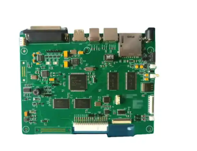
PCB, Printed Circuit Board, is a conductive board used to support and connect electronic components. It uses a copper-clad laminate as the base material, on which a circuit pattern is made through a specific process to realize the connection of electronic components and signal transmission. PCB is responsible for the connection and support functions of electronic components in electronic equipment, and is a key link in realizing the functions of electronic products.
The design and manufacturing process of PCB is relatively complex. The designer will design the circuit diagram according to the functional requirements of the circuit, and then convert the design diagram into a PCB layout diagram through electronic design automation (EDA) software. Next, processes such as chemical etching or mechanical scraping are used to remove unnecessary copper foil material from the copper-clad board, leaving only the parts required to form the circuit path. Finally, the electronic components are mounted and soldered in predefined locations to assemble the final PCB.
The main difference between copper clad laminate and PCB board
- Application scope and function: Copper clad laminate is a general material used to prepare PCB as the core component of electronic equipment. It has a wide range of applications in the electronics industry, including consumer electronics, communications, medical, aerospace and other fields. PCB is a specific product, which is made by processing copper foil on a copper-clad board.
- Structure and process: PCB is made up of multiple layers of different materials, with an insulating layer and a conductive layer in the middle, and the surface is covered with a protective film. The copper-clad laminate only has one layer of base material and one layer of copper foil, and its structure is relatively simple. In terms of process, PCB manufacturing involves multiple complex steps, including drilling, electroplating, circuit production, solder mask production, etc., while the manufacturing process of copper-clad laminates is relatively simple.
- Performance and usage: Due to different structures and processes, PCB and copper-clad laminates also differ in performance and usage. PCB has the characteristics of high integration, high density and high reliability, and can be used in various complex electronic devices, such as computers, mobile phones, TVs, etc. Copper-clad laminate is mainly used as the basic material for making single-sided or double-sided PCB, and its performance and use are relatively single.
- Price and cost: Since PCB needs to go through multiple complex process steps and material stacking, its price and cost are relatively high. The copper-clad laminate has a simple structure, simple process, and relatively low price and cost.
In summary, there are obvious differences between copper-clad laminates and PCB boards in terms of application scope and function, structure and process, performance and use, as well as price and cost.
In practical applications, appropriate materials and processes need to be selected according to specific needs to achieve the best circuit connection effect and reduce costs.