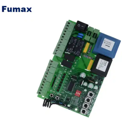
VME (VMEbus) is a computer bus standard that is widely used in aviation, aerospace, industrial control and high-end scientific computing fields.
VME PCB (printed circuit board) is a key component to implement the VME bus standard. This article will introduce the assembly and manufacturing process of VME PCB in detail.
VME PCB design stage
Before starting the assembly and fabrication of VME PCB, the circuit board design first needs to be done. The main tasks in the design phase include:
- Choose the appropriate plate material: Choose the appropriate base material according to the application requirements, such as FR4, CEM-1, etc. These materials have different electrical and physical properties, such as thermal conductivity, dielectric constant, and mechanical strength.
- Layout design: According to the circuit schematic diagram, electronic components, power supply, grounding and other elements are reasonably laid out on the circuit board. Consider factors such as component arrangement, spacing, and heat dissipation to ensure the stability and reliability of the PCB.
- Determine the wiring rules: According to the signal quality and electrical performance requirements, determine the width, spacing and number of wiring layers of the wires. Wiring rules also involve considerations such as impedance matching and signal integrity.
- Generate light drawing files: Based on the designed layout and wiring rules, generate light drawing files for subsequent PCB manufacturing. The light drawing file contains the precise location information of all wires and components on the circuit board.
VME PCB Manufacturing

The PCB manufacturing stage involves the process of converting the designed circuit diagram into an actual physical circuit board. This stage mainly includes the following steps:
- Prepare the board: Select the appropriate base material according to the design requirements, and perform cutting and drilling processes to prepare for the subsequent manufacturing process.
- Screen printing: The designed circuit pattern is transferred to the board through screen printing to form the initial shape of the wire.
- Etching: Use chemical or physical methods to remove excess copper foil to form a complete circuit pattern. This step determines the final shape and size of the wires on the PCB.
- Soldering preparation: Carry out pad processing in the area where electronic components need to be soldered so that the components can be firmly connected to the circuit board.
- Detection and Correction: Conduct quality inspection during the manufacturing process to discover and correct possible defects in a timely manner. Common inspection methods include visual inspection, X-ray inspection and flying probe inspection.
- Final inspection and packaging: After completing PCB manufacturing, conduct final quality inspection to ensure that the design requirements are met. Qualified products are packaged and ready to enter the next stage of the assembly process.
VME PCB Assembly
PCB assembly is the process of soldering electronic components to a circuit board and mainly includes the following steps:
- SMT: Place the electronic components on the corresponding positions on the PCB in the order of the layout design. This step can be done using automated equipment or manually.
- Soldering: The electronic components are connected to the pads on the PCB through a soldering process. There are many welding methods, such as wave soldering, reflow soldering, etc. Choose the appropriate welding method according to specific needs.
- Inspection and correction: Quality inspection is performed during the assembly process to ensure that the components are welded firmly and there are no short circuits or open circuits. Correct or re-weld unqualified solder joints.
- Final inspection and packaging: After completing the PCB assembly, conduct final quality inspection to ensure stable and reliable product performance. Qualified products are packaged and prepared for delivery to customers or subsequent testing, application, etc.
VME PCB Quality Control
Quality control is a crucial link throughout the entire VME PCB assembly and manufacturing process. Quality control involves strict monitoring and management of various steps to ensure that the output of each link meets preset quality standards. Quality control includes not only the inspection of the product itself, but also the monitoring and management of processes, raw materials, equipment, etc. Through continuous improvement and optimization of the production process, product quality and reliability can be continuously improved to meet customers’ high standards.
In summary, the assembly and manufacturing of VME PCB is a complex process involving multiple links. From design to manufacturing to assembly, each step requires delicate operation and management. Through strict quality control and continuous improvement, high-quality, high-performance VME PCB products can be manufactured to meet the needs of various complex applications.