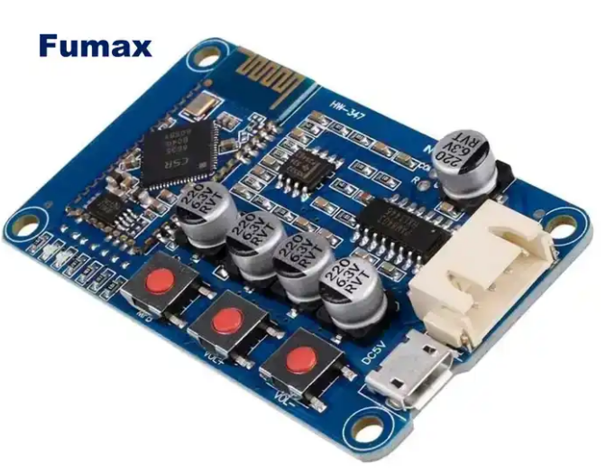
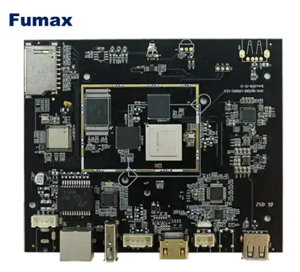
The working principle of UV machine in PCB circuit board is a complex process involving multiple physical and chemical principles.
The following is a detailed introduction to the working principle of UV machines in PCB circuit boards:
Overview

The UV machine in PCB circuit board is a device that uses ultraviolet light (UV) to cure the surface of the circuit board. UV curing technology is an efficient and environmentally friendly surface treatment technology that is widely used in PCB manufacturing, electronic packaging, liquid crystal display and other fields.

Through the irradiation of a UV machine, specific UV light energy can trigger a chemical reaction in the photosensitizer in the coating material, thereby quickly curing the coating material on the surface of the circuit board.
Working principle
- Coating materials
The key to UV curing lies in the selection of coating materials. Commonly used coating materials include epoxy resin, acrylate, polyurethane, etc. These materials can be quickly cured under UV light irradiation. Photosensitizer is added to the coating material, which is a substance that can react under UV light irradiation. The degree of reaction depends on the energy density of UV light and the irradiation time.
- UV light source
The core component of the UV machine is the UV light source, which is composed of high-power UV lamps and can emit UV light of a specific wavelength. Common UV lamps include UV-A, UV-B and UV-C bands. The UV-C band (200-300nm) has higher energy and better penetration ability, so it is widely used in UV curing technology.
- Optical path design
The optical path design in the UV machine is also one of the key factors. The purpose of light path design is to ensure that UV light can evenly illuminate the surface of the circuit board to avoid shadows or underexposure. To achieve this goal, UV machines usually use reflectors or optical lenses to focus and guide UV light. Reflectors are generally made of highly reflective materials such as aluminum and silver, which can reflect UV light to the required working area; while optical lenses can focus UV light into parallel beams or conical beams to make the light more concentrated.
- Temperature control
During the UV curing process, the increase in circuit board surface temperature is also a factor that needs to be considered. Temperatures that are too high may cause the coating material to deform or bubble, while temperatures that are too low may affect the curing effect. Therefore, UV machines are usually equipped with a cooling system to control the temperature of the circuit board surface. Common cooling methods include forced air cooling and liquid cooling, which take away heat by bringing the cooling medium (such as air, water, etc.) into direct or indirect contact with the circuit board, thereby maintaining the stability of the surface temperature of the circuit board.
- Control system
The control system is the command center for the normal operation of the entire UV machine. It is responsible for coordinating the work of various components and ensuring the smooth progress of the entire curing process. Control systems usually include power modules, control panels, sensors and actuators.
The power module is responsible for providing stable power supply; the control panel provides a human-machine interface to facilitate operator parameter setting and process monitoring; the sensor is used to detect parameters such as the position, temperature, and UV light intensity of the circuit board; the actuator is based on the control system instructions to adjust the position of the circuit board or adjust the operating status of the cooling system, etc.
Operating procedures
- Loading: Put the circuit board to be cured into the conveyor belt or fixed position.
- Coating application: Apply an appropriate amount of coating material on the surface of the circuit board by spraying, scraping, etc.
- UV irradiation: Put the circuit board into the UV machine, and guide the UV light through the reflector or optical lens to evenly illuminate the surface of the circuit board.
- Cooling: Reduce the surface temperature of the circuit board to a suitable range through the cooling system.
- Unloading: Take out the cured circuit board.
- Quality inspection: Conduct quality inspection on the cured circuit board, such as checking the coating surface quality, adhesion, etc.
- Packaging: Pack qualified products for transportation and storage.
Precautions
- The intensity and irradiation time of UV light need to be set according to the specific coating materials and process requirements to avoid poor curing effects due to insufficient or excessive light.
- During the operation, the working area should be kept clean and dry to avoid dust or water vapor from affecting the curing effect.
- Regularly inspect and maintain UV machines and related equipment to ensure their normal operation and extend their service life.
- Operators must undergo professional training and be familiar with equipment operating procedures to ensure safe and efficient completion of curing work.
- If any abnormality is discovered during operation, the machine should be stopped immediately for inspection and troubleshooting to ensure production safety and quality stability.
Future trends
With the continuous development of science and technology, UV curing technology is also constantly improving and improving. In the future, the development of UV machines will develop in the following directions:
- High efficiency: Further improve the curing speed and production efficiency of UV machines to meet the market’s growing demand for mass production. This requires the development of more efficient UV light sources and key technologies such as optimized optical path design.
- Intelligent: By introducing automation and intelligent technology, functions such as remote monitoring, fault diagnosis and adaptive control of UV machines are realized. This will help improve production efficiency and product quality, and reduce the work intensity and difficulty of operations for operators.
- Environmental protection: As environmental awareness increases, more environmentally friendly UV curing technologies and materials will receive more attention and applications. For example, we are developing coating materials with low volatile organic compounds (VOC) to reduce environmental pollution.
- Multi-functionality: On the basis of meeting the basic curing needs, add additional functions of the UV machine, such as coating surface treatment, quality inspection, etc., to improve the use value and production efficiency of the equipment.
- Customization: Customize UV machines with specific functions according to the needs of different industries and different production processes. This will help meet the diverse needs of the market and increase the application scope of UV curing technology.
Conclusion
With the continuous development of the electronics industry, UV curing technology, as one of the key links in PCB circuit board manufacturing, has broad development prospects.
Through continuous technological innovation and application expansion, UV machines will play a more important role in future industrial production.
At the same time, with the improvement of environmental protection requirements and the continuous improvement of production efficiency, UV machines will face more challenges and opportunities.
Only through continuous innovation and improvement can we meet the constant changes and demands of the market and inject new vitality into the development of the electronics industry.