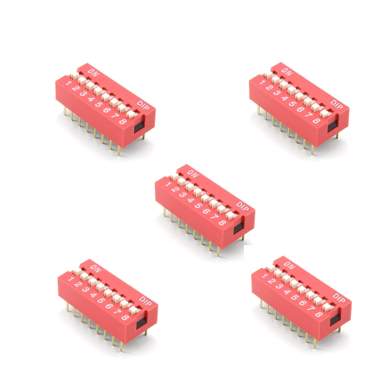
In the field of electronic manufacturing, DIP production workshop (Dual In-line Package) is a crucial part.
This important link involves soldering and assembling electronic components and is an integral step in the manufacturing of various devices and electronic products.
The following content discusses the process flow of the DIP production workshop and its importance in electronic manufacturing.
DIP welding process overview:
The DIP welding process is to insert electronic components (such as resistors, capacitors, integrated circuits, etc.) into pre-designed holes on the printed circuit board (PCB).
And fix them by soldering to form the circuit connection. This is a highly technical process that requires superb operator skills and sophisticated equipment.
Key steps in DIP production workshop:
- Component installation: First, the operator will insert the electronic components into the holes of the PCB to ensure that they are accurately aligned and positioned. The accuracy of this step is critical to the performance of the final product.
- Soldering: Once the components are properly installed, next comes the soldering process. This is usually done using wave soldering or immersion soldering techniques.
In wave soldering, the PCB is immersed in a surge of molten solder and the component pins are soldered.
In immersion soldering, pins pre-coated with solder paste are soldered using hot air or infrared heating.
- Cleaning and inspection: After completing soldering, the PCB usually needs to go through a cleaning process to remove residual solder paste or impurities.
Then, inspections are performed to ensure the quality and accuracy of the welds.
- Packaging and Labeling: Finally, the completed electronic components are packaged and labeled, ready to enter the next stage of the manufacturing process.
The importance of DIP production workshop:
DIP production workshops play a vital role in electronics manufacturing. Here are its key benefits and value:
- High reliability: The DIP welding process provides a highly reliable way to connect circuits, which is very important for applications requiring long-term stability and durability.
The high reliability of the DIP soldering process has made it a mainstay in the electronics manufacturing industry. Whether in consumer electronics, industrial applications or military fields,
DIP welding provides stable and reliable circuit connections for various electronic devices, providing a solid foundation for the successful operation of various applications.
- Wide applicability: DIP production is suitable for various PCB and electronic components, from small electronic equipment to complex industrial automation systems.
DIP production has become an important process in the electronics manufacturing industry due to its wide applicability. Not only can it be applied to various PCBs and electronic components,
It can also adapt to different application fields and performance requirements, providing reliable connection and assembly solutions for the manufacturing of various electronic devices.
- Efficiency and cost-effectiveness: This DIP welding process is generally more economical and easier to maintain and manage. The DIP production process has been carefully designed,
Designed to maximize productivity. From component insertion and soldering to cleaning and inspection, every step is optimized to reduce production cycle times and ensure orders are completed on time.
The cost-effectiveness of DIP production is outstanding. Compared with some advanced soldering technologies, such as surface mount technology (SMT), DIP production generally has lower investment and operating costs.
- Combination of tradition and modernity: Although DIP welding is a traditional technology, DIP production also makes full use of modern automation and control technology.
Advanced tools such as computer-aided design (CAD) and computer numerical control (CNC) machines are widely used to manufacture PCBs and components with precision.
DIP production inherits the reliability of traditional processes, brings excellent performance and flexibility to the electronics manufacturing industry, and provides reliable electronic component manufacturing solutions for various applications.
Conclusion:
The DIP production shop is the core of electronic manufacturing, providing reliable circuit connections and assembly. Through fine process control and high-level technology,
DIP welding process continues to promote progress in the electronic field. Its key role is to ensure the performance and reliability of electronic equipment, laying a solid foundation for our daily electronic products.