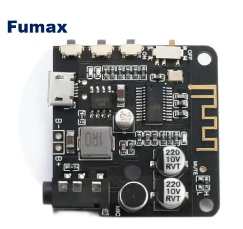
Circuit board assembly services refer to one-stop services from PCB design, PCB production, PCBA processing, and PCBA testing.
In other words, PCB assembly is a PCBA service considered from the customer’s perspective. Customers only need to provide corresponding solution documents to the manufacturer and produce product testing, allowing customers to devote themselves to new product development and sales, saving customers a lot of time and energy. and production costs.
Read the following information to learn about 4 advantages of choosing a PCBA assembly manufacturer for your next PCB manufacturing and assembly project.
- One-stop service for PCBA manufacturing: Experienced PCBA manufacturing companies provide one-stop service for PCB manufacturing. This means you don’t need to outsource PCB manufacturing to another manufacturer. Experienced PCBA manufacturers can handle everything from initial circuit board design to final product assembly. They will also take care of supply chain logistics, which has become a major issue for many electronics manufacturers.
- Save design time: PCB design time is one of the key factors in PCB assembly and manufacturing. Even if you have a talented design team, the design process can be time-consuming. Many times, a design may not serve its purpose and may require your designer to start over on a new design board. However, PCBA manufacturers will help you overcome design challenges.
- Accuracy and production speed: Shortened delivery times and product quality are two conditions for success in the electronics industry. Experienced PCBA manufacturing companies can guarantee short delivery times and accuracy with their advanced facilities. After production, they test the printed circuit boards in a real environment to avoid future failures.
- Lower component procurement costs: PCBA manufacturers have established long-term cooperative relationships with component suppliers. PCBA manufacturers often purchase components in large quantities, which helps them minimize component procurement costs. . Additionally, these industry-wide relationships help them source components easily.
Are there any benefits to designing a multilayer circuit board?
A multilayer circuit board is defined as a PCB made of three or more layers of conductive copper foil. They appear as several layers of double-sided circuit boards, laminated and glued together, with thermal insulation between them. All electrical connections between layers are made through holes, such as plated through holes, blind vias, and buried vias.
From a technical perspective, multilayer circuit boards offer several design advantages. So, what are the benefits of multilayer circuit board design?
- Small size: One of the most prominent and praiseworthy benefits of using multi-layer PCB is its size. Due to their multi-layer design, multi-layer PCBs are inherently smaller than other PCBs with similar functionality. Since the current trend is towards smaller, smaller yet more powerful gadgets, this brings major benefits to modern electronics.
- Lightweight construction: The smaller the PCB, the lighter the weight, especially since the multiple connectors required to interconnect separate single- and double-layer PCBs are eliminated in favor of a multi-layer design. Again, this is advantageous for modern electronics, which are better suited for mobility.
- High quality: Due to the amount of work and planning required to create a multi-layer PCB, these types of PCBs tend to be better in quality than single- and double-layer PCBs. As a result, they also tend to be more reliable.
- Enhanced durability: Multi-layer PCBs tend to be durable by nature. Not only do these multi-layer PCBs have to support their own weight, they also have to be able to withstand the heat and pressure that holds them together. On top of these factors, multilayer PCBs use multiple layers of insulation between circuit layers and bind them all together with prepreg adhesive and protective materials.
- More powerful: Multi-layer PCBs are extremely high-density components that integrate multiple layers into a single PCB. These nearly quarters make the board more connected, and its inherent electrical properties allow it to achieve greater capacity and speed despite its smaller size.
- Single connection point: Multi-layer PCBs are designed as a single unit rather than in series with other PCB components. As a result, they have only one connection point instead of the multiple connection points required using multiple single-layer PCBs. This is particularly beneficial for small electronics and gadgets designed to minimize size and weight.