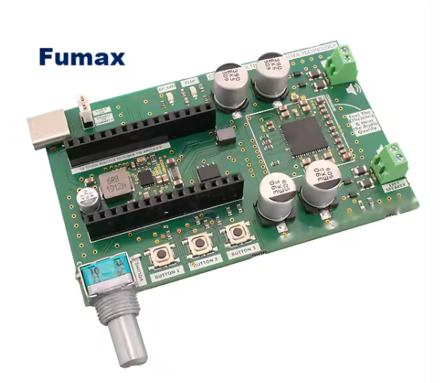
PCB reverse engineering refers to the process of starting from the finished PCB and analyzing its structure, wiring, components and other information to obtain its design drawings, schematics, BOM list and other related technical information.
It is an important technical means in the fields of electronic product design, production, maintenance, imitation and other fields.
The core principle of PCB reverse engineering is to deduce its design and manufacturing process through physical analysis and logical analysis of PCB.
Steps of PCB reverse engineering
PCB reverse engineering can generally be divided into the following steps:
- Data collection: Collect various information about PCB, including appearance, size, number of layers, materials, component models, wiring diagrams, etc.
- Physical analysis: Physical analysis of the PCB, including measuring the size, number of layers, thickness, pad diameter and other parameters of the PCB, and observing the surface process of the PCB, component packaging form, etc.
- Logic analysis: Logic analysis of PCB, including analysis of PCB circuit principles, wiring rules, signal integrity, etc.
- Modeling: Based on the analysis results, establish a PCB model, including schematic diagram, wiring diagram, BOM list, etc.
- Verification: Verify the model to ensure its accuracy.
Key Technologies of PCB Reverse Engineering
Key technologies for PCB reverse engineering include:
- PCB Image Acquisition: PCB image acquisition is the first step in PCB reverse engineering, and its purpose is to obtain a clear image of the PCB. Commonly used PCB image acquisition methods include scanning, photography, X-ray, etc.
- PCB Image Processing: PCB image processing is the second step of PCB reverse engineering. Its purpose is to enhance the quality of PCB images and extract the structure and wiring information of PCB. Commonly used PCB image processing methods include image enhancement, edge detection, segmentation, etc.
- PCB component identification: PCB component identification is an important step in PCB reverse engineering. Its purpose is to identify the models and parameters of all components on the PCB. Commonly used PCB component identification methods include manual identification, machine learning, etc.
- PCB circuit analysis: PCB circuit analysis is the core step of PCB reverse engineering. Its purpose is to analyze the circuit principles and wiring rules of PCB. Commonly used PCB circuit analysis methods include manual analysis, circuit simulation, etc.
- PCB Modeling: PCB modeling is the last step of PCB reverse engineering. Its purpose is to establish a model of PCB, including schematic diagram, wiring diagram, BOM list, etc. Commonly used PCB modeling software includes Altium Designer, Cadence Allegro, etc.
Application of PCB reverse engineering

PCB reverse engineering has a wide range of applications, mainly including the following aspects:
- Product Design: Through PCB reverse engineering, you can obtain technical information of competitors’ products and provide reference for your own product design.
- Product Imitation: Existing products can be quickly copied through PCB reverse engineering, reducing product development costs.
- Fault Analysis: PCB reverse engineering can analyze the causes of PCB failures and find solutions.
- Intellectual Property Protection: Through PCB reverse engineering, you can analyze the technical solutions of competitors’ products and take measures to protect your own intellectual property rights.
Precautions for PCB reverse engineering
PCB reverse engineering is a complex technology. When performing PCB reverse engineering, you should pay attention to the following matters:
- Comply with relevant laws and regulations: PCB reverse engineering may involve intellectual property issues, therefore, relevant laws and regulations should be observed when performing PCB reverse engineering.
- Pay attention to PCB confidentiality: PCB may contain sensitive information, therefore, when performing PCB reverse engineering, you should pay attention to PCB confidentiality.
- Have professional knowledge and skills: PCB reverse engineering requires certain professional knowledge and skills. Therefore, PCB reverse engineering should be performed by professionals.
Summarize
PCB reverse engineering is a powerful technique that can provide people with a lot of valuable information.
However, PCB reverse engineering may also be used for illegal purposes. Therefore, when using PCB reverse engineering technology, you should pay attention to comply with relevant laws and regulations.