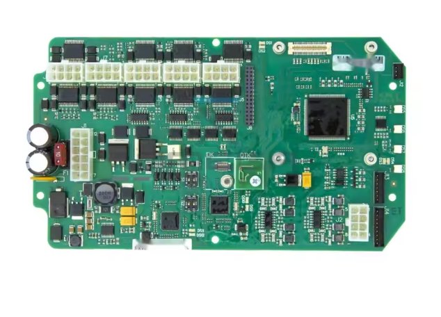
DIP (Dual Inline Package) packaging in SMT (Surface Mount Technology) processing is a form of electronic component packaging, mainly used for packaging of integrated circuits (ICs).

DIP packages feature side-by-side metal pins on both sides of the component, which are used to solder the IC chip to the circuit board.
This packaging form was very common in early electronic manufacturing, but with the advancement of technology, other more advanced packaging forms (such as SOP, SSOP, QFP, BGA, etc.) gradually replaced DIP packaging.
The following is a detailed introduction to DIP packaging in SMT processing:
Basic principles and characteristics of DIP packaging
The basic principle of DIP packaging is to encapsulate the integrated circuit chip in a plastic or ceramic shell. There are several metal pins on both sides of the shell for connection with external circuits. DIP packages are characterized by a higher pin count and are typically used for integrated circuits that require higher pin counts.
In addition, DIP packaging has good mechanical strength and high reliability, so it is widely used in some situations that require high stability.
Application of DIP packaging in SMT processing
In SMT processing, DIP packaging is mainly used to solder integrated circuit chips to circuit boards. SMT processing uses automated production lines, and components are accurately mounted on circuit boards through placement machines, welding machines and other equipment. DIP packaged integrated circuits can be fixed to the circuit board through special DIP sockets or soldering. During the welding process, appropriate welding processes and welding materials need to be used to ensure welding quality and reliability.
Advantages and limitations of DIP packaging
(1) Advantages
- High mechanical strength: DIP packaging has good mechanical strength and can resist external impact and vibration.
- High reliability: DIP packaging has high reliability and is suitable for applications that require high stability.
- Easy to repair and replace: Due to the large number of pins in the DIP package, damaged integrated circuits are easy to repair and replace.
(2) Limitations
- Limited number of pins: The number of pins in DIP packaging is limited by the package size, and is generally not suitable for integrated circuits with too many pins.
- Large space occupation: DIP packaged integrated circuits are larger in size and occupy more circuit board space.
- Not suitable for high-density assembly: With the continuous miniaturization and thinning of electronic products, DIP packaging has gradually been unable to meet the needs of high-density assembly.
Manufacturing process and quality control of DIP packaging
(1) Manufacturing process
- Chip preparation: Select the appropriate integrated circuit chip and perform necessary testing and screening.
- Pin production: According to the packaging requirements, make the appropriate number and length of pins.
- Packaging: Put the chip and pins into the packaging mold, inject the packaging material (such as plastic or ceramic), and then perform curing, cutting and other processes to form a DIP packaged integrated circuit.
- Testing and screening: Test and screen the packaged integrated circuits to ensure that the quality meets the requirements.
(2) Quality control
- Material selection: Use high-quality packaging materials and pin materials to ensure packaging quality and reliability.
- Process control: Strictly control parameters such as temperature, pressure, and time during the packaging process to ensure stable packaging quality.
- Inspection and testing: Comprehensive inspection and testing of packaged integrated circuits, including appearance inspection, electrical performance testing, etc., to ensure that product quality meets requirements.
Market prospects and technology development trends of DIP packaging
With the continuous advancement of electronic technology and consumers’ increasing performance requirements for electronic products, the market demand for DIP packaging has gradually weakened. However, in some specific fields, such as military, aerospace and other occasions that require extremely high stability and reliability, DIP packaging still has a certain market share.
In terms of technology development trends, with the continuous advancement of integrated circuit manufacturing processes and innovation in packaging technology, more advanced and compact packaging forms have gradually become mainstream. In the future, DIP packaging may be replaced by more advanced packaging forms (such as WLCSP, FOWLP, etc.). At the same time, with the rapid development of smart manufacturing and the industrial Internet, the level of automation and intelligence in SMT processing will continue to improve, providing better technical support for the production and application of DIP packaging.
Summarize
In general, DIP packaging, as a traditional integrated circuit packaging form, has certain application value in SMT processing. However, with the advancement of technology and changes in market demand, the market share and technical status of DIP packaging may gradually decrease. Therefore, electronics manufacturing companies need to pay close attention to market dynamics and technology development trends, and promptly adjust production strategies and technical routes to adapt to the changing market demands and technical environment.
The above content introduces DIP packaging in SMT processing in detail, including its basic principles, characteristics, applications, advantages and limitations, manufacturing process and quality control, as well as market prospects and technology development trends. It is hoped that these contents can help readers better understand and apply DIP packaging technology.