In the electronics manufacturing industry, ensuring the quality and functionality of Printed Circuit Board Assemblies (PCBAs) is crucial. One of the key tools used in this process is the PCBA testing jig. This article will provide an in-depth overview of what a PCBA testing jig is, its basic structure, how it is manufactured, and how it is used. This comprehensive guide aims to shed light on the importance of PCBA testing jigs in maintaining the integrity and reliability of electronic products.
What is a PCBA Testing Jig?
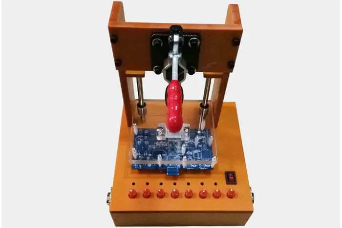
A PCBA testing jig, also known as a test fixture, is a specialized device used to test the functionality and performance of PCBAs. These jigs are essential in the manufacturing process as they allow for the efficient and accurate testing of electronic circuits. By simulating real-world conditions, PCBA testing jigs help identify any defects or issues in the assembly, ensuring that only high-quality products move forward in the production line.
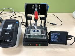
PCBA testing jigs can be customized to fit specific requirements and can vary significantly in complexity. From simple mechanical fixtures to advanced automated systems, these jigs are designed to interface with the PCBA and test various parameters such as voltage, current, resistance, and signal integrity.
Basic Structure of a PCBA Testing Jig
The basic structure of a PCBA testing jig consists of several key components:
- Fixture Base: The foundation of the testing jig, which holds all other components in place. It is usually made from durable materials such as aluminum or steel to ensure stability and longevity.
- Probes: These are the contact points that interface with the PCBA to measure electrical signals. Probes can be spring-loaded pins, needles, or other types of connectors, depending on the specific requirements of the test.
- Connector Interface: This part connects the testing jig to external test equipment such as multimeters, oscilloscopes, or automated test systems. It ensures that the signals from the PCBA are accurately transmitted to the measurement devices.
- Clamping Mechanism: A system to securely hold the PCBA in place during testing. This can include clamps, vacuum systems, or other types of fixtures that prevent movement and ensure consistent contact between the probes and the PCBA.
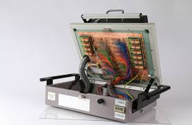
- Control Electronics: In more advanced testing jigs, control electronics are used to automate the testing process. This can include microcontrollers, relays, and other components that manage the sequence of tests and record the results.
How PCBA Testing Jigs are Manufactured
Manufacturing a PCBA testing jig involves several steps:
- Design: The first step is to design the jig based on the specific requirements of the PCBA. This involves creating a detailed schematic that outlines the placement of probes, the clamping mechanism, and the connector interface. Computer-Aided Design (CAD) software is commonly used for this purpose.
- Prototype Development: Once the design is finalized, a prototype of the jig is developed. This allows for testing and verification of the design to ensure it meets the necessary specifications. Any issues identified during this phase are addressed before moving to mass production.
- Material Selection: Choosing the right materials is crucial for the durability and performance of the jig. High-quality metals and plastics are selected based on factors such as mechanical strength, electrical conductivity, and thermal stability.
- Machining and Assembly: The individual components of the jig are machined and assembled. This involves precise manufacturing techniques such as CNC machining, laser cutting, and 3D printing. The components are then assembled according to the design specifications.
- Testing and Calibration: The assembled jig is thoroughly tested and calibrated to ensure it functions correctly. This includes verifying the alignment of probes, checking the connectivity of the interface, and validating the control electronics.
- Quality Control: A final quality control check is performed to ensure that the jig meets all necessary standards and specifications. This step is crucial to guarantee the reliability and accuracy of the testing jig.
How to Use a PCBA Testing Jig
Using a PCBA testing jig involves several steps:
- Setup: Begin by setting up the testing jig on a stable surface. Ensure that all necessary connections to external test equipment are securely made. This includes connecting the jig to power supplies, measurement devices, and any control systems.
- Loading the PCBA: Carefully place the PCBA onto the jig, ensuring that it is properly aligned with the probes and securely held by the clamping mechanism. This step is crucial to ensure accurate test results.
- Performing the Test: Initiate the testing process according to the specified procedures. This may involve running automated test sequences or manually performing measurements. The testing jig will simulate various conditions and measure the PCBA’s response.
- Recording Results: Record the results of the tests, noting any deviations from the expected values. Advanced testing jigs may automatically log this data for further analysis.
- Analyzing Data: Analyze the test results to identify any issues or defects in the PCBA. This may involve comparing the measured values against predetermined thresholds or running diagnostic software.
- Taking Corrective Actions: If any issues are identified, take the necessary corrective actions. This may involve reworking the PCBA, adjusting the manufacturing process, or refining the testing jig.
- Re-testing: After making any necessary corrections, re-test the PCBA to ensure that the issues have been resolved. Repeat the testing process as needed to verify the quality and functionality of the assembly.
Conclusion
PCBA testing jigs are indispensable tools in the electronics manufacturing industry. They play a crucial role in ensuring the quality and reliability of PCBAs by providing a means to accurately test and validate their performance. By understanding the basic structure, manufacturing process, and usage of these jigs, manufacturers can better appreciate their importance and implement effective testing strategies.
Investing in high-quality PCBA testing jigs and following best practices in their use can significantly enhance the overall quality of electronic products, leading to increased customer satisfaction and reduced costs associated with defects and rework. Whether you are a manufacturer or an engineer, having a solid grasp of PCBA testing jigs is essential for success in the ever-evolving field of electronics.