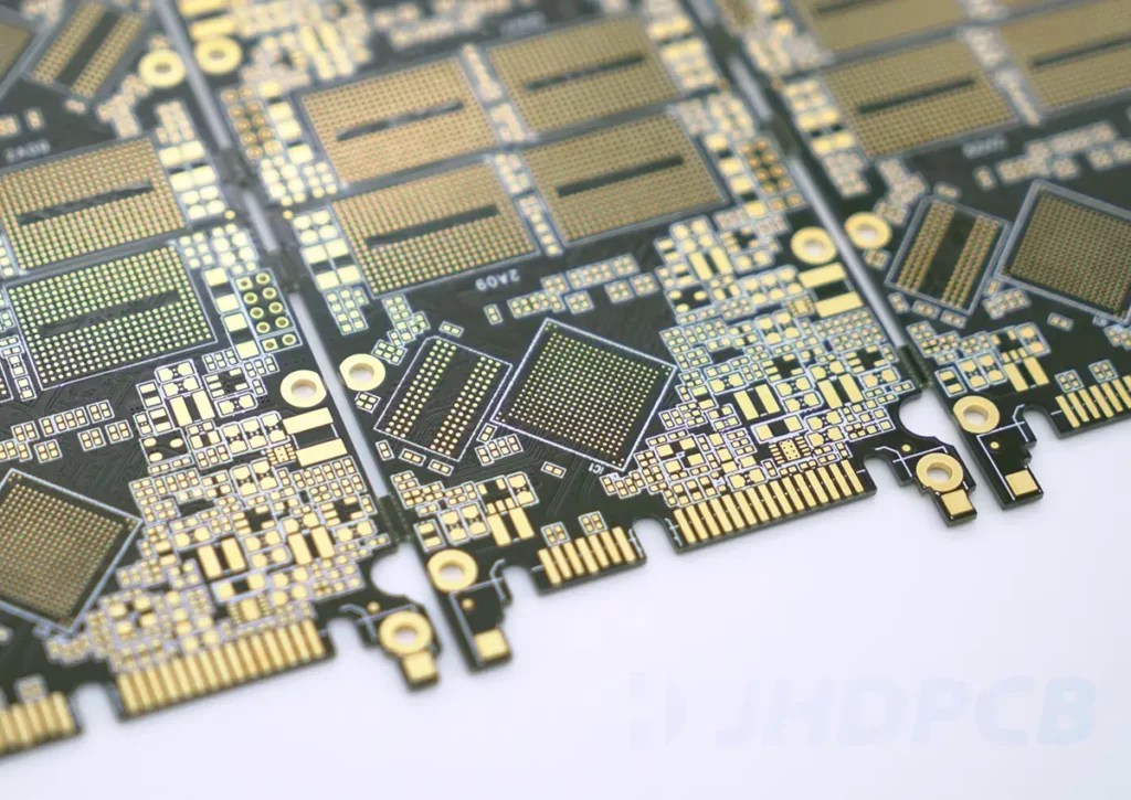
Multi-layer PCBs (Printed Circuit Boards) are widely used in modern electronic devices due to their capability to provide more routing layers, higher electrical performance, and reduced size. However, assembling multi-layer PCBs involves several critical steps and meticulous attention to detail to ensure the final product’s quality and reliability. Below are the detailed considerations to keep in mind during the multi-layer PCB assembly process.
1. Manufacturing Phase Considerations
Material Selection and Quality Control:
- High-Quality Substrates: Choose appropriate substrates such as FR4, high-TG materials, ceramics, or polyimide to ensure the mechanical strength and thermal stability of the multi-layer PCB.
- Copper Thickness: Select the suitable copper thickness according to the current carrying requirements, typically 1oz/ft² or 2oz/ft².
Lamination Process and Alignment:
- Lamination Temperature and Pressure: Control the temperature and pressure during the lamination process to ensure the adhesion strength and uniformity between layers.
- Interlayer Alignment: Precisely align each layer to prevent misalignment, which can cause electrical shorts or open circuits.
Drilling and Plating Process:
- Drilling Precision: Use high-precision drilling equipment to ensure that the holes’ positions and sizes meet the design requirements.
- Plating Quality: Control the current and time during the plating process to ensure a uniform copper layer on holes and pads without defects.
Etching and Cleaning:
- Etching Process: Control the etching speed and time to ensure the clarity and accuracy of the circuit patterns.
- Residue Cleaning: Thoroughly clean the chemical residues and impurities on the PCB surface to prevent them from affecting subsequent soldering and assembly.
2. Assembly Phase Considerations
Soldering Techniques:
- Reflow Soldering: Select the appropriate reflow soldering temperature profile based on the thermal sensitivity of the components. Precisely control the preheat, soldering, and cooling stages to avoid excessive temperatures that could cause PCB warping or delamination.

- Wave Soldering: For through-hole components, ensure proper wave soldering parameters to avoid solder bridging. Maintain the soldering time and temperature within reasonable limits to prevent damage to the lower layers.
Component Placement and Soldering:
- Component Orientation and Polarity: Strictly follow the design documents during component placement to ensure the correct orientation and polarity, preventing soldering errors.
- Solder Joint Inspection: Inspect each solder joint visually or with automated optical inspection (AOI) to ensure smooth and defect-free solder joints.
Testing and Inspection:
- Electrical Testing: Conduct comprehensive electrical tests, including continuity and isolation tests, functional tests, and signal integrity tests, to ensure every circuit and component works correctly.
- X-ray Inspection: Use X-ray inspection to check the internal layer solder joints and via fillings, ensuring no internal defects.
- Functional Testing: Perform full functional testing after assembly to verify that each component and circuit operates as intended.
Environmental Control:
- Electrostatic Discharge (ESD) Protection: Implement strict ESD protection measures during assembly and testing, using ESD-safe workbenches, wrist straps, and flooring to prevent damage to sensitive components.
- Clean Environment: Maintain a clean assembly area using cleanrooms or clean workbenches to prevent dust and contaminants from affecting the PCB.
Protection Coatings and Packaging:
- Selecting Appropriate Coatings: Choose suitable protection coatings like conformal coatings, potting compounds, or protective films based on the product’s usage environment to enhance the PCB’s environmental resistance and reliability.
- Uniform Coating Application: Ensure an even application of the coating, avoiding excessively thick or thin layers that could impact the PCB’s electrical performance and heat dissipation.
Labeling and Marking:
- Barcodes and Serial Numbers: Add barcodes or serial numbers to the PCB for traceability in production batches and quality control.
- Clear Markings: Ensure clear markings for each component and test point to facilitate subsequent testing and repair.
Packaging and Transportation:
- Moisture-Proof Packaging: Use moisture-proof packaging materials to prevent moisture ingress after assembly.
- Shock-Proof Packaging: Protect the PCB with shock-proof packaging materials during transportation to safeguard it from physical impacts and vibrations.
Thermal Management During Assembly:
- Component Layout: Strategically place heat-generating components and heat sinks to ensure effective thermal management and avoid hotspots.
- Thermal Vias: Design thermal vias under high-heat components to improve heat conduction from the component to the heat dissipation layers.
Handling and Storage:
- Proper Handling Procedures: Follow proper handling procedures to avoid mechanical damage, contamination, and ESD damage.
- Storage Conditions: Store PCBs in controlled environments with appropriate temperature and humidity levels to prevent oxidation and moisture absorption.
Solder Paste Application:
- Stencil Quality: Use high-quality stencils for precise solder paste application. Ensure the stencil apertures are clean and correctly aligned with the PCB pads.
- Solder Paste Inspection: Inspect the solder paste deposition to ensure correct volume and coverage on each pad, preventing solder bridges and insufficient solder joints.
Component Placement Accuracy:
- Pick-and-Place Machine Calibration: Regularly calibrate pick-and-place machines to ensure accurate component placement.

- Component Alignment: Verify component alignment before reflow soldering to avoid misalignment and placement errors.
Post-Assembly Cleaning:
- Flux Residue Removal: Thoroughly clean flux residues after soldering to prevent corrosion and electrical leakage.
- Cleaning Process Control: Use controlled cleaning processes with appropriate solvents and equipment to ensure effective cleaning without damaging the PCB.
Rework and Repair:
- Rework Procedures: Establish standardized rework procedures for addressing assembly defects or component failures.
- Repair Documentation: Document all rework and repair activities to maintain traceability and ensure quality control.
Conclusion
The assembly of multi-layer PCBs is a complex process that requires meticulous attention to detail at every stage. From material selection and manufacturing to assembly and testing, each step involves specific considerations to ensure the final product’s performance and reliability. By adhering to these detailed considerations, manufacturers can achieve high-quality multi-layer PCBs that meet the stringent requirements of modern electronic devices. Ensuring strict quality control throughout the entire process is essential to delivering reliable and efficient PCB assemblies.