There are many SMT chip processing factories in China. Below, fumax will introduce to you the companies that specialize in SMT processing and production in China. fumax is a professional SMT processing factory and PCBA custom assembly factory in China.
The top 5 SMT patch processing factories in China are as follows:
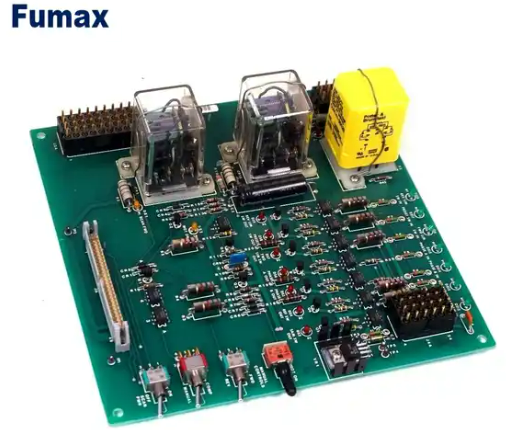
1.Fumax
Circuit board PCBA design and custom development, PCB board, PCBA, aluminum substrate, flexible line PCB board, software programming, component procurement, SMT patch processing, PCBA OEM, DIP welding, assembly testing and painting, etc. BOM procurement One-stop service provider. It has nearly 20 years of rich industry experience and complete production and testing equipment.
A high-tech enterprise specializing in SMT chip processing services.
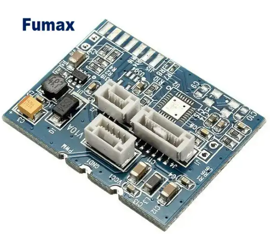
Its main business includes SMT patch processing, PCBA patch processing, etc., which are widely used in communications, consumer electronics, automobiles and other fields. Fumax is a national high-tech enterprise.
Our company address is in Nanshan District, Shenzhen, China, and the PCBA and PCB manufacturing factories are in Fuyong Street, Bao’an District, Shenzhen, China.
- Guangdong Huazhuang Technology Co., Ltd. Guangdong Huazhuang Technology Co., Ltd. is a national high-tech enterprise engaged in diversified electronic manufacturing services such as EMS/OEM/JIT. Its main products involve communication equipment, medical electronics, automotive electronics, industrial control electronics, new energy and other fields.
- Shenzhen Jingwang Electronics Co., Ltd.: This company is a high-tech enterprise specializing in the R&D, production and sales of electronic components and modules. Its main products include electronic components, LED lighting, automotive electronics, communication electronics, etc. The company has advanced production equipment and a complete quality management system to provide customers with high-quality, high-reliability products and services.
- Xiamen Liding Optoelectronics Co., Ltd.: This company is a high-tech enterprise specializing in the research, development, production and sales of optical lenses and optoelectronic products. Its main products include various types of optical lenses, optoelectronic products and peripheral products, which are widely used in mobile phones, cameras, automobiles, security and other fields. The company has advanced production equipment and an excellent R&D team to provide customers with high-quality products and services.
- Shenzhen Jinyida Electronics Co., Ltd. is a high-tech manufacturer specializing in PCB boards, PCBA, PCB circuit boards, aluminum substrates, flexible circuit boards, and PCB proofing. It provides single-sided, double-sided, multi-layer circuit board samples and mass production, and provides steel Network, one-stop service for SMT patches and components.
The process of SMT chip processing factory of Chinese PCB manufacturers
The process of the SMT patch processing plant mainly includes steps such as solder paste printing, dispensing, patching, curing, reflow soldering, X-RAY inspection, wave soldering, manual quality inspection, cleaning, board splitting and packaging for shipment.
Among them, solder paste printing is to print solder paste or patch glue through the steel mesh onto the pads of the PCB to prepare for the welding of components; dispensing is to drip glue onto the fixed position of the PCB to fix the components. onto the PCB board; patching is to accurately install the surface-mounted components to the fixed position of the PCB; curing is to melt the patch adhesive so that the surface-mounted components and the PCB board are firmly bonded together; reflow soldering is to apply the solder paste Melting, the surface assembly components and the PCB board are firmly bonded together; X-RAY inspection is to detect the components on the PCB board to ensure their correct installation; wave soldering is to solder the PCB board through a wave soldering machine; Manual quality inspection performs manual quality inspection on the PCB board after wave soldering to ensure the welding quality; cleaning is to clean the PCB board and equipment to remove residual dirt and solder; depaneling is to divide the PCB board into different parts so that Subsequent processing; packaging and shipping is to package PCB boards and components into finished products and prepare them for shipment.
In SMT patch processing, it is difficult to fix FPC for high-precision mounting, and it is difficult to ensure consistency during mass production, which requires high equipment. For the fixation of FPC, the entire process from printing and patching to reflow soldering needs to be fixed on a pallet, and the pallet used requires a small thermal expansion coefficient. There are two fixing methods. Method A is used when the QFP lead spacing is above 0.65MM. The pallet is placed on the positioning template. The FPC is fixed on the pallet with thin high-temperature resistant tape, and then the pallet is separated from the positioning template for printing. Method B is used when the QFP lead spacing is less than 0.65MM. The pallet is placed on the positioning template, the FPC is fixed on the pallet with high-temperature resistant tape, and then the pallet is separated from the positioning template for printing. The high-temperature resistant tape used should have a moderate viscosity, must be easy to peel off after reflow soldering, and must have no adhesive residue on the FPC.
The above information is for reference only. If necessary, please contact the staff of our SMT chip processing factory.