Today we will introduce the process flow analysis of DIP plug-in and DIP plug-in processing. In PCB assembly, DIP is a packaging method of integrated circuits; it is part of the PCBA (PCB assembly) process.
What does DIP plug-in processing mean?
DIP plug-in processing means that the processing manufacturer processes the PCB board according to the documents and materials required for processing provided by the customer, inserts electronic components such as resistors, capacitors, diodes, pin headers, etc. into the correct position, and performs wave soldering, etc. A general term for a series of processes.
Dual in-line packaging (DIP) is a packaging method for integrated circuits and is also a part of the PCBA (Printed Circuit Board Assembly) process. This packaging method is characterized by a double row of pins and a small package width (height).
After SMT (Surface Mount Technology) patch processing, the DIP plug-in process is part of the PCBA process. Plug-ins refer to large-sized components that cannot be mounted by machines and need to be plugged in manually and then soldered through wave soldering. The plug-in process can be roughly divided into plug-in, wave soldering, clipping, inspection, testing and other processes.
As chip processing equipment becomes more and more advanced, PCBs and electronic components become smaller and smaller, and SMT chip processing has a tendency to gradually replace DIP plug-in processing. However, as an important link in the PCBA process, the quality of the DIP plug-in determines the quality of the PCBA processing. Therefore, it is very necessary to understand the relevant knowledge of plug-in holes.
When processing DIP plug-ins, attention needs to be paid to controlling parameters such as temperature, time, conveyor belt speed, and flux to ensure welding quality and efficiency. At the same time, there are a variety of modes for making plug-in holes, including Circle Drill, Oval Slot, Rectangle Slot, etc. This knowledge is very necessary for those who perform DIP plug-in processing.
DIP plug-in processing process
The process flow of DIP plug-in processing mainly includes the following steps:
- Plug-in: Insert the processed components into the corresponding position on the PCB board to prepare for wave soldering.
- Wave soldering: Put the plugged-in PCB board into the wave soldering conveyor belt, and complete the soldering of the PCB board through flux spraying, preheating, wave soldering, cooling, etc.
- Component leg cutting: Cut the legs of the welded PCBA board to achieve the appropriate size.
- Repair welding (post-welding): PCBA finished boards that are not completely welded must be repaired and repaired.
- Board washing: Clean the harmful substances such as flux remaining on the finished PCBA to meet the environmental cleanliness standards required by customers.
During the processing of DIP plug-ins, you also need to pay attention to the following points:
- Pre-processing: After receiving the materials, carefully check the material model and specifications, and perform pre-production pre-processing according to the template.
- Material baking: Chips, PCB boards, modules and special materials that have been in stock for more than 3 months must be baked at a high temperature of 120℃ for 24H. Objects that are not resistant to high temperatures such as MIC microphones and LED lights must be baked at 60℃ 24H low temperature baking.
- Component molding and processing: Use automatic bulk capacitor shearing machine, automatic transistor molding machine, fully automatic belt molding machine and other molding equipment for processing.
In general, only by complying with these steps and precautions can the quality and efficiency of DIP plug-in processing be guaranteed to the greatest extent.
What should we pay attention to during wave soldering during DIP plug-in processing?
In the process flow of DIP plug-in processing, wave soldering is an important link. The following points need to be paid attention to:
- Temperature and time: Wave soldering requires controlling the preheating temperature and time, as well as the wave soldering temperature and time. If the temperature is too high or the time is too long, it may cause component damage or PCB board damage.
- Conveyor belt speed: The speed of the conveyor belt will affect the welding effect. If the speed is too fast, it may cause poor welding or missed soldering. If the speed is too slow, the components may be overheated and damaged.
- Flux: Flux is an essential substance for wave soldering. If too much flux is used, the surface of components or PCB boards may be contaminated, affecting the soldering effect.
- Component placement: Before wave soldering, the components need to be placed correctly in the corresponding position on the PCB board. If the components are placed improperly, it may lead to poor welding or failure to weld.
- Cleaning: After wave soldering, the PCB board needs to be cleaned to remove residual flux and other impurities on the surface to ensure the cleanliness and quality of the PCB board.
In short, during the wave soldering process, it is necessary to pay attention to many aspects such as temperature, time, conveyor belt speed, flux, component placement and cleaning to ensure welding quality and efficiency.
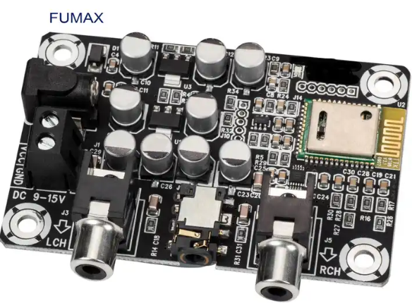
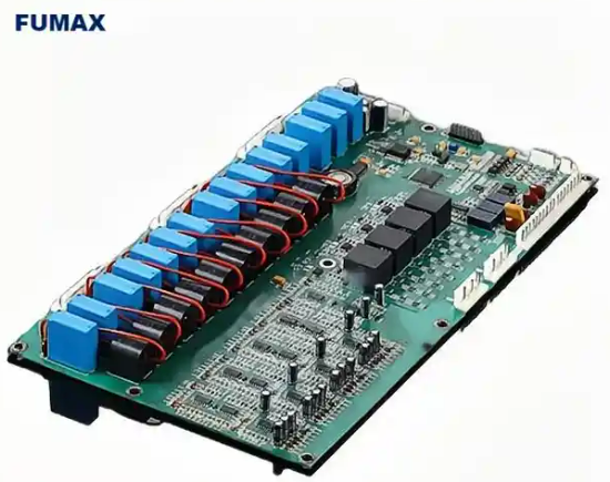
Single-sided DIP plug-in PCB assembly factory in China
Fumax is a well-known company among single-sided DIP plug-in PCB assembly factories in China. Shenzhen Fumax Technology Co., Ltd., referred to as Fumax, is a comprehensive enterprise integrating PCB R&D, manufacturing, sales and service.
Fumax has rich experience and professional technology in the field of PCB manufacturing, and is committed to providing customers with high-quality, high-efficiency PCB solutions. Its products are widely used in automotive electronics, communication equipment, control systems, medical equipment and other fields.
Fumax has advanced production equipment and manufacturing technology, focuses on quality management, and has passed ISO9001 quality management system certification. Formai has also established a complete technology research and development system, owns a number of patented technologies, and continuously improves its technical level and innovation capabilities.
In short, Fumax, as a single-sided DIP plug-in PCB assembly factory, has won widespread customer recognition and market share with its professional technology, high-quality products and good services.