LED (Light Emitting Diode), as an efficient and environmentally friendly lighting device, has been widely used in various fields.
As the support and connection structure of LED devices, LED PCB’s assembly quality and defect analysis have an important impact on the performance and reliability of LED devices. This article will introduce in detail the assembly process of LED PCB and analysis of common defects.
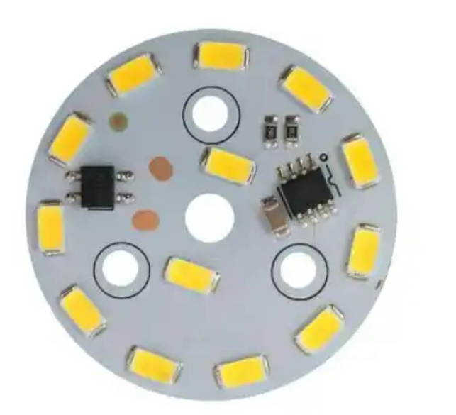
LED PCB assembly process
- Prepare materials
Before assembling the LED PCB, you need to prepare the required materials, including LED devices, PCB boards, solder, flux, etc. Ensure all materials are of the required quality and specifications.
- Clean the PCB board
Before assembly, the PCB board needs to be cleaned to remove dust, oxides and other impurities on the surface. This helps improve weld quality and reliability.
- Solder the LED device
Weld the LED device to the PCB board to ensure that the welding quality is good and there are no welding, cold welding, etc. At the same time, pay attention to the direction and position of the LED device to ensure that it is aligned with the pads on the PCB board.
- Testing and Debugging
After completing the assembly, testing and debugging are required to ensure the normal function of the LED PCB. The test content includes the brightness, color, direction, etc. of the LED device, as well as the electrical performance and stability of the PCB board.
Analysis of common defects of LED PCB
- Virtual soldering
Welding is one of the common defects in the LED PCB assembly process. Welding may cause the connection between the LED device and the PCB board to be unstable, affecting the performance and reliability of the LED device. The reasons for weak soldering may include too low soldering temperature, too short soldering time, poor soldering quality, etc. In order to prevent false soldering, it is necessary to control the soldering temperature and time and select high-quality solder materials.
- Cold welding
Cold welding refers to defects caused by the failure of the solder to fully melt due to the temperature being too low or the time being too short during the welding process. Cold welding may cause poor connection between the LED device and the PCB board, affecting the performance and reliability of the LED device. In order to prevent cold welding, the welding temperature and time need to be controlled to ensure that the solder fully melts and fills the pad.
- Dislocation
Misalignment refers to the incorrect position or wrong orientation of the LED device during the welding process. Misalignment may lead to poor connection between the LED device and the PCB board, affecting the performance and reliability of the LED device. In order to prevent misalignment, the orientation and position of the LED device need to be carefully checked before assembly to ensure that it is aligned with the pads on the PCB board.
- Short circuit
Short circuit refers to a poor or incorrect connection between the LED device and the PCB board, resulting in a short circuit of current. A short circuit may cause damage to the LED device or failure of the entire circuit system. In order to prevent short circuits, it is necessary to ensure that the connection between the LED device and the PCB board is stable and reliable to avoid connection errors or poor contact.
- Oxidation
Oxidation refers to the appearance of oxides on the surface of LED devices or PCB boards, resulting in poor connections or performance degradation. Oxides may affect the conductivity and stability of LED devices. In order to prevent oxidation, measures need to be taken to prevent the LED device and PCB board from being exposed to the air, such as using antioxidants or taking other protective measures.
in conclusion
LED PCB assembly quality and defect analysis have an important impact on the performance and reliability of LED devices. In order to improve product quality and reliability, it is necessary to strictly control the welding temperature and time during the assembly process, select high-quality solder materials, carefully check the direction and position of the LED device, and other measures. At the same time, corresponding preventive measures and treatment methods need to be taken for common defects such as virtual welding, cold welding, misalignment, short circuit and oxidation. By strengthening quality control and management measures, the assembly quality and reliability of LED PCB can be effectively improved.