introduction
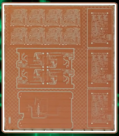
With the continuous development of electronic technology, PCB boards have become an indispensable part of modern electronic equipment.
In the application of testing SPI and temperature sensors, the design and production of PCB boards are particularly important. This article will introduce in detail the manufacturing method of PCB board for testing SPI and temperature sensor, including design, board making, welding and other steps.
design

- Determine the design plan
In the design stage, the PCB board design plan needs to be determined based on the specific needs of testing SPI and temperature sensors. Including board selection, layout, wiring, component packaging, etc. At the same time, issues such as heat dissipation and anti-interference also need to be considered.
- Design using EDA tools
Use professional EDA tools (such as Altium Designer, Eagle, etc.) for PCB board design. In EDA tools, operations such as component layout, wiring, and component packaging can be easily performed. At the same time, EDA tools also provide a wealth of libraries and tools to facilitate designers to design.
- Export design files
After the design is completed, the design file needs to be exported as a Gerber file or PDF file. These files will be used for subsequent board making and welding.
Board making
- Choose the right board
Select the appropriate plate material based on the design plan and testing requirements. Commonly used plates include FR4, CEM-1, aluminum substrate, etc. Different boards have different properties, such as heat resistance, corrosion resistance, thermal conductivity, etc. Therefore, when choosing a plate, you need to make a choice based on the actual situation.
- Make light painting film
Import the design file into the light plotter to create a light painting film. Light-painting film is a mask used to make PCB boards, and its quality directly affects the production quality of PCB boards. Therefore, when making light painting films, it is necessary to ensure their quality and accuracy.
- Make PCB board
The light-painted film is attached to the substrate, and after exposure, development, etching and other steps, a PCB board is produced. During the production process, attention needs to be paid to controlling parameters such as temperature and time to ensure the production quality and accuracy of the PCB board.
welding
- Component welding
Solder components such as SPI and temperature sensor to the PCB board. Before welding, the components need to be pre-processed, such as cleaning, tin plating, etc. At the same time, it is also necessary to select appropriate welding materials and welding processes to ensure welding quality and reliability.
- Debugging and testing
After completing the soldering, the PCB board needs to be debugged and tested. Through debugging and testing, you can ensure the normal operation of components such as SPI and temperature sensors, as well as the stability and reliability of the PCB board. At the same time, the PCB board can also be optimized and improved to improve its performance and reliability.
Summarize
This article introduces in detail the manufacturing method of PCB board for testing SPI and temperature sensor, including design, board making, welding and other steps. Through the introduction of this article, you can understand that the design and production of PCB boards is a complex and meticulous work that requires comprehensive consideration of multiple factors. At the same time, with the continuous development of electronic technology, the design and production of PCB boards will continue to progress and improve.
Frequently Asked Questions and Answers about PCB Board Production for Testing SPI and Temperature Sensors
When making PCB boards for testing SPI and temperature sensors, you may encounter some common problems. Here are some possible problems and their solutions:
- PCB short circuit:
Reason: The biggest cause of PCB short circuit is improper soldering pad design. In addition, improper design of PCB part direction, automatic plug-in bent legs, too large substrate holes, too low solder furnace temperature, poor board solderability, solder mask failure, board contamination, etc. can also cause short circuits.
Solution: You can change the circular pad to an oval shape to increase the distance between points to prevent short circuits. The direction of the part can also be appropriately modified to make it perpendicular to the tin wave to avoid short circuits. - Dark and granular contacts appear on the PCB board:
Reason: Dark or granular contact problems appear on the PCB, mostly because the solder is contaminated and there are too many oxides mixed into the molten tin, resulting in a solder joint structure that is too brittle.
Solution: Pay attention to check the quality of the solder and ensure cleanliness during the soldering process to reduce the mixing of oxides.