Eight major processes of HDI PCB production

HDI (High Density Interconnect) production is a complex process involving multiple steps and links. The following provides you with an overview of the eight major processes of HDI PCB production. The details of each process will be gradually expanded according to your needs.

HDI production and production eight major processes:

HDI design

In the HDI production process, design is the crucial first step. This stage involves the use of professional software to create circuit diagrams and layouts to meet the needs of specific applications. Designers need deep knowledge of electronic engineering in order to correctly realize the circuit function and optimize the layout.

HDI original production

After completing the design, enter the prototype production stage. This step involves the use of laser cutting or other methods to cut the design from flexible substrates to form the basic structure of the circuit. This stage is essential to verify the correctness and integrity of the design.
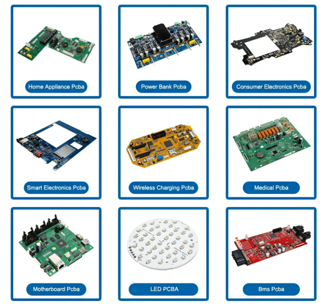
Eight major processes of HDI PCB production

HDI electroplating

After the prototype is completed, electroplating is needed to increase the conductivity and improve the durability of the circuit. During the electroplating process, a layer of metal will be deposited on the surface of the circuit, such as copper or nickel to improve the electrical performance.

HDI exposure

Exposure is a very important link in HDI production. It involves light using a specific wavelength to illuminate the sensor to form a circuit pattern. This process is usually used to complete the exposure machine to ensure the accuracy and clarity of the pattern.

HDI show

After exposure, enter the show stage. In this step, the uncovered photosensitive material will be removed, and the exposure part will be retained to form a circuit pattern. This process needs to accurately control the composition and time of the developed solution to ensure the quality of the pattern.

HDI etching

After the development is completed, etching is required. The etching process uses chemical reagents to remove the non -pattern part of the material to form a accurate circuit structure. This step is essential to ensure the integrity and accuracy of the circuit.

HDI peeling

After the etching is completed, the peeling treatment is usually performed. In this step, the remaining photosensitive materials and other auxiliary materials will be removed, leaving only the final circuit structure. This process needs to accurately control the ingredients and time of the stripping solution to ensure the quality and stability of the circuit.

HDI test

The last step is testing and testing. At this stage, the HDI board needs to perform a series of tests to ensure that its performance and quality meet the requirements.

Test items may include electrical performance testing, appearance inspection, reliability testing, etc. Once the test is passed, the HDI board can be delivered to the customer.

The above is an overview of the eight major processes produced by HDI. Each process has its specific technical requirements and quality control standards, and it is necessary to strictly observe to ensure the quality and reliability of the final product.

In actual production, these processes are usually completed by professional teams, and team members must have knowledge and skills in related fields. If you need the detailed content of each process or have a deeper understanding of a specific process, please provide demand, we will continue to write for you.

Related Posts

HDI PCB’s Advantages in Industrial electronics

Why HDI and how does it work In the realm of industrial control systems, High-Density Interconnect (HDI) Printed Circuit Boards (PCBs) have emerged as transformative components, revolutionizing the landscape of modern manufacturing and automation. HDI PCBs play a pivotal role in enhancing the functionality, reliability, and compactness of various industrial devices, facilitating an era of […]

Introduction to IPC Standards in PCB Manufacturing and Assembly

The IPC (Association Connecting Electronics Industries) is a global trade association that develops standards for the electronics manufacturing industry. These standards are crucial for ensuring quality, reliability, and consistency in the production of printed circuit boards (PCBs) and their assembly. This article will cover the main IPC standards relevant to PCB manufacturing and assembly, detail […]

Solder Paste, Rosin, and Flux: Differences and Which One to Use?

Why Rosin and Flux Help with Soldering Rosin and flux make soldering easier for a few key reasons: How They Work Rosin: When heated, it decomposes into active components that remove oxides and form a protective gas to prevent further oxidation. Flux: Contains various active ingredients that become active at high temperatures, cleaning oxides, improving […]

How to design PCB for IoT Products with UWB Modules

Designing PCBs for Internet of Things (IoT) products, especially those incorporating Ultra-Wideband (UWB) modules, involves a unique set of challenges and considerations. These include ensuring optimal electrical performance, thermal management, mechanical strength, manufacturability, environmental compliance, and cost-effectiveness. This article delves into the specific factors engineers need to consider when designing PCBs for IoT products with […]

Understanding Motors: Types, Control PCB Design, and Top 10 Chinese Manufacturers

What are Motors and Their Types? Motors are essential devices that convert electrical energy into mechanical energy, powering countless applications from household appliances to industrial machinery. Understanding the different types of motors is crucial for selecting the right one for your needs. Here are the main types of motors: Designing and Producing Motor Control PCBs […]

Multi-layer PCB Assembly Guideline in 2024

Multi-layer PCBs (Printed Circuit Boards) are widely used in modern electronic devices due to their capability to provide more routing layers, higher electrical performance, and reduced size. However, assembling multi-layer PCBs involves several critical steps and meticulous attention to detail to ensure the final product’s quality and reliability. Below are the detailed considerations to keep […]

Introduction to PCBA Testing Jigs

In the electronics manufacturing industry, ensuring the quality and functionality of Printed Circuit Board Assemblies (PCBAs) is crucial. One of the key tools used in this process is the PCBA testing jig. This article will provide an in-depth overview of what a PCBA testing jig is, its basic structure, how it is manufactured, and how […]

Unveiling Circuit Card Assembly 2024: From PCB Manufacturing to Board Assembly

Hey there, tech enthusiasts! Get ready to dive deep into the fascinating world of circuit card assembly. In this comprehensive guide, we’ll take you through every meticulous step of the process, from PCB manufacturing to the final assembly of the board. So grab your coffee, settle in, and let’s explore the intricate journey of bringing […]

Optimizing High-Speed Design: Balancing Signal, Power, and EMC for Success

Editor’s Note: In modern high-speed designs, analyzing signal integrity, power integrity, and EMC separately is not enough; a holistic approach is essential for successful design. Background Issue: When signals cross over segmentation areas between adjacent reference planes on a layer, discussions about signal integrity often arise. Some argue that signals should not cross the segmentation […]