The design and assembly of solar PCB boards is a complex process involving multiple fields.
The following is a detailed introduction to solar PCB board design and assembly, covering all aspects from design concept to actual assembly.
Overview
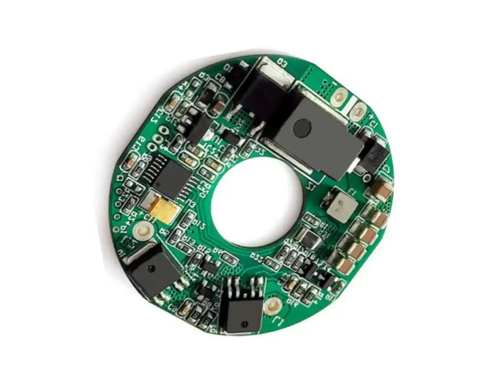
Solar PCB board, also known as solar power control board, is an electronic device that converts solar energy into DC power. Its core part is the solar cell component, which converts light energy into electrical energy through the photoelectric effect or photochemical effect. Solar PCB boards are widely used in distributed photovoltaic power generation systems, solar lamps, solar water heaters and other fields.
Solar PCB board design
- Need analysis
Before starting the design, it is necessary to clarify the product requirements, including output voltage, current, power, size, cost, etc. - Circuit design
Carry out circuit design based on demand analysis. It mainly includes the following parts:
(1) Main circuit design: The main circuit is responsible for storing the electric energy generated by the solar panel into the battery or directly supplying it to the load. Select the appropriate rectifier, inverter and charging circuit according to the characteristics and needs of the load.
(2) Control circuit design: The control circuit is responsible for monitoring the photovoltaic panel output voltage, battery power, load status and other information, and adjusting the working status of the main circuit according to the actual situation to ensure efficient and stable operation of the system.
(3) Protection circuit design: The protection circuit is used to prevent system overload, overvoltage, undervoltage, overcurrent and other abnormal conditions from causing damage to the system. - Layout design
Layout design refers to the reasonable layout of various circuit components on the PCB board to improve the reliability, maintainability and aesthetics of the product. In layout design, the arrangement, spacing, routing, etc. of components need to be considered. - Electromagnetic compatibility design
Since solar PCB boards work in an outdoor environment, they are easily affected by lightning, electromagnetic interference and other factors. Therefore, electromagnetic compatibility needs to be considered in the design and corresponding measures should be taken to reduce the impact of electromagnetic interference on the system. - Thermal design
Thermal design is an important part of ensuring the stable operation of solar PCB boards under long-term working conditions. During the design process, factors such as the amount of heat generated by each component and the way of heat dissipation need to be considered to ensure good heat dissipation performance of the system. - Reliability design
Since solar PCB boards need to work in harsh environments for a long time, reliability design is required. During the design process, it is necessary to consider the impact of environmental factors, mechanical stress and other factors on product reliability, and take corresponding measures to improve product reliability. - Maintainability design
Maintainability design refers to taking the maintainability of the product into consideration during the design process to facilitate later maintenance and upkeep. During the design process, factors such as maintenance convenience and spare parts replacement need to be considered. - Design review and optimization
After completing the preliminary design, a design review is required to evaluate and optimize the design plan. The review content mainly includes circuit principles, layout, electromagnetic compatibility, thermal design, reliability, maintainability, etc. Based on the review results, the design plan will be optimized and improved.
Solar PCB board assembly
- Material preparation
According to the design plan, prepare the required electronic components, structural parts, auxiliary materials and other materials. During the material preparation process, the quality and reliability of the materials need to be strictly controlled to ensure that the performance of the assembled products is stable and reliable. - PCB board processing
Send the designed PCB board to the processing factory for processing, including pad processing, component mounting, welding and other processes. During the processing, the processing quality needs to be strictly controlled to ensure that the electrical and mechanical properties of the PCB board meet the requirements. - Assembly process
(1) Component mounting: Mount electronic components on the PCB board according to process requirements. During the mounting process, attention needs to be paid to parameters such as the direction, position, and mounting pressure of components to ensure that component mounting is firm and reliable.
(2) Welding: Use welding technology to connect electronic components to PCB boards. During the welding process, attention must be paid to the welding temperature, welding time and solder quality to ensure that the welding quality meets the requirements.
(3) Quality inspection: Conduct quality inspection on the assembled PCB board, including electrical performance testing, appearance inspection and functional testing, etc. Unqualified PCB boards need to be repaired or scrapped. - Finished product assembly and testing
Fix the welded PCB board to the corresponding structural parts and assemble the finished product. During the assembly process, attention needs to be paid to the reliability of the mechanical properties and electrical properties of the product. After assembly is completed, the product needs to be comprehensively tested, including functional testing, performance testing and environmental adaptability testing. Ensure that the product meets the design requirements and can work stably and reliably. - Packaging and Shipping
Packaging and transportation are carried out according to product characteristics and customer requirements. During the packaging process, care needs to be taken to protect the product from factors such as vibration, shock, and moisture. At the same time, appropriate transportation methods and transportation routes need to be selected to ensure that products can be delivered to customers safely and timely. - Document organization and maintenance
During the design and assembly process, relevant documents need to be organized and maintained, including design plans, circuit schematics, layout drawings, welding process documents, etc. These documents are important materials in the product development process and are of great significance for subsequent product maintenance and upgrades. At the same time, documents need to be backed up and updated regularly to ensure their completeness and accuracy. - Personnel training and safety protection
During the design and assembly process, attention needs to be paid to personnel training and safety protection. Through regular technical training and safety