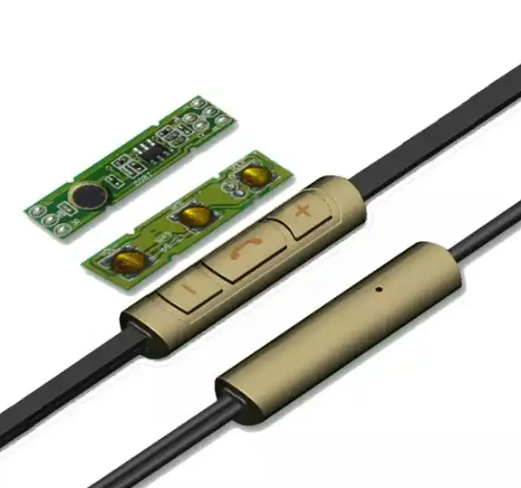
Metalized Printed Circuit Board (MCPCB) refers to a circuit board in which one or more layers of metal are deposited on a copper-clad board (FR-4) to form a circuit pattern.
MCPCB has the advantages of high conductivity, high reliability, corrosion resistance, etc., and is widely used in electronic products, electrical equipment, automobiles and other fields.

The manufacturing process of MCPCB mainly includes the following steps:
PCB cutting
Cutting refers to the process of cutting the original copper-clad laminate into boards that can be produced on the production line. It is generally cut into work boards of about 40*50cm. Cutting generally uses mechanical methods, such as cutting machines, laser cutting machines, etc.
Drilling
Drilling refers to drilling the holes required for circuits on the work board. Generally, the diameter of the drilled holes ranges from 0.1mm to 10mm. The quality of drilling directly affects the performance and reliability of the circuit board. Drilling generally uses mechanical methods, such as electric spark drills, ultrasonic drills, etc.
Hole metallization
Hole metallization refers to depositing a layer of copper on the drilled work board to connect the various layers of circuits. Hole metallization generally uses chemical deposition or electrochemical deposition.
Chemical Deposition
Chemical deposition refers to a method that uses chemical reactions to deposit metal on the surface of a substrate. The process flow of chemical deposition hole metallization is as follows:
- Clean the work board
The purpose of cleaning the work plate is to remove oil, dust and other impurities on the surface of the work plate to ensure the quality of hole metallization. Cleaning generally uses chemical cleaning methods, such as alkaline cleaning, acid cleaning, etc.
- Electroless copper plating
Electroless copper plating refers to a method of depositing copper on the surface of a substrate using chemical reactions. The reaction formula of electroless copper plating is as follows:
CuSO4 + 2NaOH + H2O → Cu(OH)2 + Na2SO4
Cu(OH)2 + H2O → Cu + 2OH
Electroless copper plating generally uses a tank electroplating method, that is, the work board is immersed in a copper plating tank, and then an electric current is passed through to reduce the copper ions on the surface of the work board into copper.
Electrochemical Deposition
Electrochemical deposition refers to a method that uses electrochemical reactions to deposit metal on the surface of a substrate. The process flow of electrochemical deposition hole metallization is as follows:
- Clean the work board
The purpose of cleaning the work plate is to remove oil, dust and other impurities on the surface of the work plate to ensure the quality of hole metallization. Cleaning generally uses chemical cleaning methods, such as alkaline cleaning, acid cleaning, etc.
- Electroplated copper
Electroplating copper refers to a method of depositing copper on the surface of a substrate using electrochemical reactions. The reaction formula for electroplating copper is as follows:
CuSO4 + 2H2O + 2e → Cu + SO42- + 2H+Copper electroplating generally uses the electroplating bath method, that is, the work board is immersed in a copper plating bath, and then current is passed through to reduce the copper ions on the surface of the work board into copper.
Deburring and removing slag
After drilling, burrs and slag will be produced on the edge of the hole in the work plate, which needs to be removed. Deburring generally uses mechanical methods, such as grinding wheels, electric sparks, etc., while deburring generally uses chemical methods, such as alkaline cleaning, acid cleaning, etc.
Circuit graphics transfer
Circuit pattern transfer refers to the process of transferring circuit patterns to the work board. Circuit pattern transfer generally uses photolithography or screen printing.
Photolithography
Photolithography refers to a method that uses optical principles to transfer circuit patterns to a work board. The steps of photolithography are as follows:
- Coating photoresist
Photoresist is a photosensitive material that undergoes a chemical reaction when exposed to light. The purpose of applying photoresist is to protect the unexposed areas of the work board.
- Exposure
Exposure refers to the process of using a light source to transfer circuit patterns to photoresist. Exposure generally uses ultraviolet exposure.