Phenolic PCB paper substrate manufacturing and assembly focuses on high-quality circuit board production and assembly.
It uses advanced phenolic resin materials and undergoes precise manufacturing processes to ensure product reliability and stability.
Phenolic PCB paper substrate manufacturing and assembly: detailed explanation of process flow and technology
Overview of Phenolic PCB Paper Substrate Manufacturing and Assembly
Phenolic PCB paper substrate is a commonly used electronic circuit board substrate and is widely used in the manufacturing of electronic products because of its good insulation, heat resistance and corrosion resistance.
This article will provide a detailed introduction to the manufacturing and assembly process of phenolic PCB paper substrate, aiming to help readers better understand this field.
Phenolic PCB paper substrate manufacturing process
- Raw material preparation: The raw materials required to manufacture phenolic PCB paper substrates mainly include phenol, aldehyde, fillers, plasticizers, etc. Before manufacturing, raw materials need to be quality checked to ensure they meet relevant standards.
- Ingredients and premixing: Mix the main ingredients such as phenol and aldehyde according to the predetermined formula, and add appropriate amounts of fillers, plasticizers and other auxiliary ingredients. The purpose of premixing is to distribute the ingredients evenly to facilitate subsequent processing operations.
- Pressing and forming: Put the pre-mixed materials into the press and press and form at a certain temperature and pressure. During the pressing process, the material undergoes processes such as hot melting, flow and solidification, and finally forms a phenolic PCB paper substrate.
- Cooling and cutting: The pressed phenolic PCB paper substrate needs to be cooled and shaped, and then cut as needed to obtain the required size and shape.
- Quality inspection and packaging: Conduct quality inspection on the finished phenolic PCB paper substrate, including inspection of appearance, size, performance, etc. Qualified products are packaged for subsequent assembly.
Phenolic PCB paper substrate assembly process
- Drilling and hole processing: According to the needs of circuit design, use a drilling machine to drill holes on the phenolic PCB paper substrate to insert the pins of electronic components. After drilling, reaming, repairing and other processing operations may be required to ensure the quality of the holes.
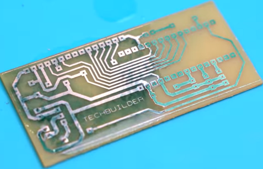
- Metallization treatment: In order to make the phenolic PCB paper substrate have good conductive properties, the drilled substrate needs to be metallized. Commonly used metallization methods include chemical copper plating and electroplating copper, so that the copper layer covers the hole wall to facilitate subsequent circuit production.
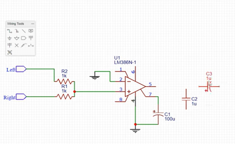
- Circuit production: On the metallized substrate, circuit patterns are produced through printing, photolithography, electroplating and other processes. This step is a key step in determining the function of the PCB and requires precise control of process parameters to ensure the quality of the circuit.
- Mount electronic components: According to the design requirements, insert the pins of the electronic components into the holes of the phenolic PCB paper substrate and weld and fix them. This step requires ensuring that the mounting position of the components is accurate and the welding quality is reliable.
- Inspection and maintenance: After completion of mounting, perform functional testing and performance testing on the assembled phenolic PCB paper substrate to ensure its normal operation. Carry out timely repairs and adjustments for detected faults or problems.
- Packaging and storage: Qualified products are packaged to protect the phenolic PCB paper substrate from damage during transportation and storage. At the same time, select appropriate packaging materials and methods as needed to ensure product safety.
Technology Outlook
With the development of the electronics industry, the performance requirements for phenolic PCB paper substrates are also constantly increasing. In the future, the manufacturing and assembly technology of phenolic PCB paper substrates will develop towards higher precision, higher reliability and more environmental protection. At the same time, new materials and technologies will continue to emerge, providing more possibilities for the manufacturing and assembly of phenolic PCB paper substrates.
Phenolic PCB paper substrate manufacturing and assembly conclusion
The manufacturing and assembly of phenolic PCB paper substrates is a complex process involving multiple process steps.
By in-depth understanding of its manufacturing and assembly processes, the technical points and difficulties in this field can be better grasped.
At the same time, paying attention to industry development trends and technological innovation is also crucial to continuously improving manufacturing and assembly levels.
Only in this way can we better meet market demand and promote the development of the electronics industry.
Fumax PCB Assembly and Manufacturing Factory
The business of phenolic PCB paper substrate manufacturing and assembly manufacturers includes electronic design, PCB layout, PCB R&D, production and sales of phenolic PCB paper substrate, providing full services from raw materials to finished products. Professional PCB OEM service.
Fumax PCB assembly manufacturers adopt advanced production technology and strict quality control to ensure product performance and reliability and meet the needs of different fields.
At the same time, Fumax PCB manufacturers also provide personalized customization services, designing and producing products according to the specific needs of customers.