The production process of assembling a single-sided PCB board includes film production, copper-clad board cutting, drilling, cleaning, flux coating, patching, welding, inspection, testing and packaging.
By strictly controlling the quality of each link, we ensure that the performance and reliability of the final product meet the requirements.
The production process of assembling a single-sided PCB board involves multiple complex steps. Here is a detailed introduction:
Single-sided PCB board production process flow
- Make film: Make film according to the designed circuit diagram. Film is a transparent plastic sheet coated with a layer of photosensitive material. The circuit diagram will be drawn on the film, and then the film will be exposed to make the circuit diagram appear on the film.
- Copper-clad board cutting: Cut the large copper-clad board into appropriate small pieces. The size of each copper-clad board must comply with the size requirements of the PCB board.
- Drilling: Drill holes in the copper-clad board so that components can be inserted into the holes. The location of these holes should correspond to the location of the components on the circuit diagram.
- Cleaning: Use chemical reagents or mechanical methods to clean the copper clad laminate to remove dirt and grease on the surface.
- Apply flux: Apply flux where soldering is required to help the soldering process go smoothly.
- SMT: Place the components on the copper-clad board according to the position on the circuit diagram. This step can be accomplished using a manual or automatic placement machine.
- Welding: Connect the components to the copper-clad board through welding. The welding process can be done using manual welding or automatic welding equipment.
- Inspection: After completing the welding, the PCB board needs to be carefully inspected to ensure that all components have been installed correctly and that there are no problems such as virtual soldering or short circuit.
- Test: Functionally test the PCB board to ensure it is working properly.
- Packaging: Pack qualified PCB boards for transportation and storage.
Process details of single-sided PCB board
- Make film: Use professional drawing software to draw the circuit diagram on the computer based on the circuit diagram provided by the customer, and then output it to the film. The thickness and transparency of the film will affect the production quality of the PCB board.
- Copper-clad board cutting: Fix the large piece of copper-clad board on the cutting machine and cut it according to the pre-designed size. During the cutting process, care must be taken to prevent problems such as burrs and breakage.
- Drilling: The purpose of drilling holes in the copper-clad board is to insert components into the holes to facilitate welding and assembly. When drilling holes, you need to pay attention to the accurate position and depth of the holes without deviation.
- Cleaning: The purpose of cleaning is to remove dirt and grease on the surface of the copper clad laminate to facilitate flux coating and welding. When cleaning, care must be taken not to damage the surface of the copper clad board.
- Apply flux: Apply flux where soldering is required to help the soldering process go smoothly. When applying, be careful not to apply too much or too little, otherwise it will affect the welding effect.
- SMT: Place the components on the copper-clad board according to the position on the circuit diagram. This step can be accomplished using a manual or automatic placement machine. When patching, care must be taken to prevent components from shifting or misaligning.
- Welding: Connect the components to the copper-clad board through welding. The welding process can be done using manual welding or automatic welding equipment. When welding, you need to pay attention to parameters such as temperature, time and pressure of the welding head to avoid problems such as virtual welding and short circuit.
- Inspection: After completing the welding, the PCB board needs to be carefully inspected to ensure that all components have been installed correctly and that there are no problems such as virtual soldering or short circuit. Tools such as a magnifying glass or microscope are required to assist observation during inspection.
- Test: Functionally test the PCB board to ensure it is working properly. When testing, you need to pay attention to the selection of test environment and test methods to ensure the accuracy and reliability of test results.
- Packaging: Pack qualified PCB boards for transportation and storage. When packaging, you need to pay attention to protecting the surface of the PCB board to prevent problems such as collisions and scratches. At the same time, attention should also be paid to the implementation of moisture-proof, dust-proof and other measures to ensure the quality and life of the PCB board.
Precautions for the production process of single-sided PCB boards
- When making films, ensure the accuracy and clarity of the circuit diagram to avoid affecting subsequent processing.
- When cutting copper-clad boards, ensure the accuracy and neatness of cutting to avoid affecting the assembly and aesthetics of the PCB board.
- When drilling holes, ensure the accuracy of the position and depth of the holes to avoid affecting the insertion and welding effects of components.
- When cleaning the copper-clad board, choose appropriate cleaning agents and cleaning methods to avoid damaging the surface of the copper-clad board or affecting its conductive properties.
- When applying flux, the coating amount and uniformity must be controlled to avoid affecting the welding effect and product quality.
- When patching, ensure the accuracy of the position and direction of components, so as not to affect the assembly and aesthetics as well as the performance and reliability of the product.
- When welding, it is necessary to control the welding temperature and time as well as the pressure of the welding head and other parameters to avoid problems such as virtual welding and short circuit that affect product quality and reliability.
- During inspection, check carefully and comprehensively to ensure that all components are installed correctly and welded well without defects.
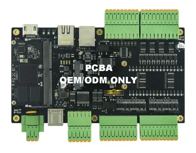
Fumax single-sided pcb board assembly manufacturer
There are many manufacturers that assemble single-sided PCB boards. Some of these large companies have advanced production equipment and leading technology and can provide high-quality PCB boards and excellent services.
At the same time, some small and medium-sized manufacturers also focus on the production and assembly of PCB boards and have corresponding professional capabilities and experience.
Fumax focuses on one-stop services such as PCB assembly, PCB manufacturing, PCB design, and PCB layout.