LED driver PCB design and assembly solution: A comprehensive guide from requirements analysis, PCB design, component selection to actual assembly, designed to ensure an efficient and reliable LED lighting system.
LED driver PCB design and assembly overview
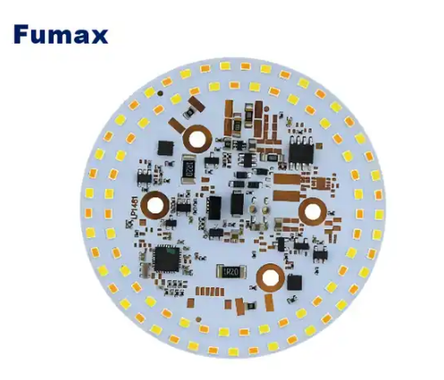
The LED driver PCB (Printed Circuit Board) is a key part of the LED lighting system and is responsible for converting power into a stable current suitable for LEDs.
High-quality PCB design can ensure system reliability, stability and security. This guide will introduce the design and assembly scheme of LED driver PCB in detail to help you build an efficient LED driver system from scratch.
LED driver PCB design stage
- Determine the requirements: Clarify the requirements of the LED system, including the required brightness, power, color and size. At the same time, understand the specifications of LEDs, such as voltage drop, current and optimal operating temperature.
- Choose the right PCB material: Choose the right PCB material according to your needs and working environment. Commonly used PCB materials include FR4, CEM-1 and aluminum substrates, etc. Each material has its specific electrical properties and heat resistance.
- Design layout: Based on the requirements and circuit schematic diagram, start designing the PCB layout. Ensure the shortest traces between components to reduce heat accumulation, while taking into account factors such as anti-interference and heat dissipation.
- Determine PCB size: Determine the size of PCB based on requirements and number of components. Make sure the PCB is the right size, too large or too small will affect its performance and cost.
- Component selection and layout: Select appropriate electronic components, such as capacitors, inductors, diodes and ICs, etc., and layout the components on the PCB according to the circuit schematic diagram. Take into account the packaging form and pin spacing of the components to ensure that they can be successfully mounted on the PCB.
- Wiring design: Carry out PCB wiring design based on the circuit schematic diagram and component layout. When wiring, factors such as current size, signal transmission speed, and electromagnetic interference need to be considered, and appropriate line widths and spacing should be used.
- Verification and optimization: Use professional PCB design software to verify the design to ensure the correctness and reliability of the circuit. Optimize the design based on the verification results, such as adjusting component locations, modifying wiring, etc.
- Generate manufacturing files: Export the designed PCB files into manufacturing files, usually Gerber files and drilling files. After checking that the manufacturing documents are correct, they are delivered to the PCB manufacturer for production.
LED driver PCB assembly stage
- Prepare components: According to the designed PCB layout, prepare all required electronic components and ensure that their quality and specifications meet the requirements.
- Soldering: Use appropriate soldering tools and techniques to solder the components to the PCB according to the layout on the PCB. Pay attention to temperature and time control during the welding process to prevent damage to components and pads.
- Check the welding quality: After the welding is completed, carefully check the welding quality of each component to ensure that there are no weak welds, missing welds, etc.
- Test: Functionally test the assembled LED driver PCB, including power access, power on and off and other functions. Make sure the system is working properly and there are no obvious abnormalities.
- Aging test: The assembled LED drive system is subjected to an aging test to simulate long-term operation under actual working conditions. Observe whether the system is stable and reliable, and discover potential problems in a timely manner.
- Cleaning and finishing: Clean the PCB surface to remove welding residue and other dirt. Organize all cables and connectors to ensure a neat and tidy appearance.
- Packaging and transportation: According to actual needs, select appropriate packaging materials and methods to ensure that the LED drive system is not damaged during transportation. At the same time, the necessary labels and precautions should be marked on the packaging.
- Documentation and maintenance: Provide complete operation and maintenance documentation, including circuit schematics, component lists, instructions for use and maintenance guides, etc. Ensure users can properly use and maintain the system.
LED driver PCB design and assembly considerations
- Safety First: Always pay attention to safety issues, especially when welding and working with high voltage equipment. Follow safety regulations and wear protective equipment.
- Comply with laws and regulations: Ensure that all components, materials and processes used comply with relevant laws, regulations and environmental protection requirements.
- Continuous learning and improvement: Continuously learn and explore new design and assembly technologies to improve your skills. At the same time, the design and assembly solutions are continuously improved and optimized based on actual experience and user feedback.
The advantages and disadvantages of LED driver PCB design and assembly solutions are as follows:
advantage:
High-efficiency performance: able to provide stable current to ensure uniform brightness and long life of the LED.
Energy saving and environmental protection: LED drive circuit has high efficiency, reduces energy waste, and the materials are recyclable.
Optimize heat dissipation: Choosing appropriate PCB materials and design layout according to needs will help improve the heat dissipation performance of the system.
Easy to maintain: PCB design makes the component layout clear and easy to detect and repair.
High integration: PCB can integrate multiple functions, reduce external connection cables, and reduce costs.
shortcoming:
Higher cost: High-quality PCB design and assembly requires a lot of time and money.
High process requirements: PCB design and manufacturing require certain professional skills and experience to ensure quality and reliability.
Customized requirements: Customized design and assembly are required according to specific needs, and mass production is not possible.
Environmental impact: A certain amount of waste will be generated during the PCB manufacturing process, and environmental protection measures need to be taken for disposal.
The above content is for reference only. It is recommended to choose the most suitable solution based on actual needs and budget.