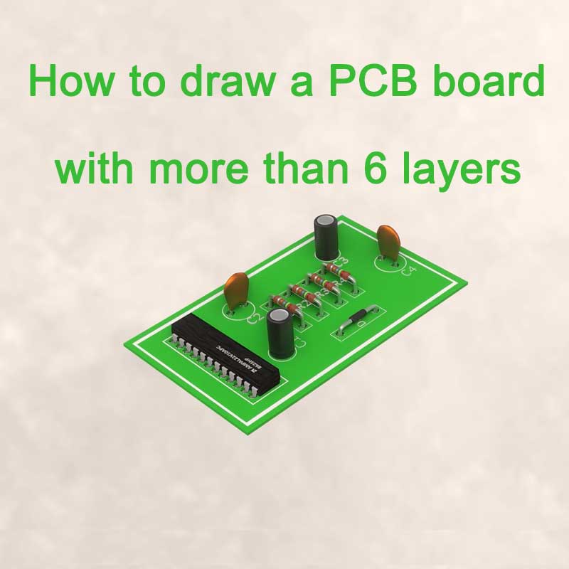
Drawing a PCB with more than 6 layers is a technical challenge that requires fine craftsmanship and strict quality control to ensure the stability and reliability of the circuit.
This multi-layer PCB board is widely used in high-end electronic equipment, providing a reliable solution for complex circuit design.
How to draw a PCB board with more than 6 layers

Drawing a PCB with more than 6 layers is a complex task that requires professional skills. The following is a detailed introduction to some steps and precautions:
Determine design requirements
Before starting design, you need to clearly understand the product requirements, including circuit functions, performance parameters, special processes, etc. At the same time, manufacturability in actual production needs to be taken into consideration to ensure that the design can be produced smoothly.
Determine the number of layers and layout
Determine the number of layers and layout required based on the complexity and manufacturability requirements of the circuit. Generally speaking, the number of layers to consider for PCB boards with more than 6 layers is 6-8 layers, and each layer has different functions and wiring requirements. During layout, factors such as signal flow, power distribution, and component placement need to be considered to ensure the rationality and manufacturability of the design.
Determine materials and processes
Select appropriate materials and processes based on design needs and layer number requirements. High-precision and high-performance PCB boards require the selection of high-precision materials and advanced processes, such as using materials with high thermal conductivity and low expansion coefficient, laser drilling, copper electroplating and other processes.
Layered design
Before starting the design, the circuit board needs to be divided into different layers, each layer has its own specific functions and wiring requirements. Generally speaking, the top and bottom layers are signal layers, and the middle layer is the power layer or ground layer.
When designing in layers, factors such as signal flow, power distribution, and component placement need to be considered to ensure the rationality and manufacturability of the design.
Wiring design
Wiring is one of the most important aspects of drawing a PCB board and needs to be carried out according to the circuit diagram and wiring rules. When designing, you need to consider the signal transmission path, resistance, capacitance, inductance and other parameters, as well as the connection relationship between components. When wiring, you can use manual or automatic wiring, choose according to the actual situation.
Add components and annotations
After the design is completed, components need to be added to the PCB board and necessary annotations and symbols added. When adding components, factors such as the component’s packaging form, number of pins, and arrangement need to be considered. At the same time, labels and symbols should be clear, accurate, concise, and easy to read and maintain.
Inspection and modification
After completing the design, careful inspection and modification are required to ensure the rationality and manufacturability of the design.
Checks include wiring connectivity, impedance matching, signal integrity, power integrity and electromagnetic compatibility.
If there is a problem that needs to be modified, you can use undo, redo, modify and other commands to operate.
Export the file and deliver it for production
Finally, the design file needs to be exported to a format acceptable to the board manufacturer (such as Gerber file), and the file format conversion and delivery must be performed according to the requirements of the board manufacturer.
At the same time, it is necessary to communicate with the board manufacturer to ensure that the produced PCB boards meet the design requirements and quality standards.
The above is a detailed introduction to the general steps and precautions for drawing PCB boards with more than 6 layers. It should be noted that other factors may need to be considered in actual operation, such as the size, shape, weight, etc. of the PCB board.
At the same time, continuous optimization and improvement are needed to improve design level and production efficiency.
If you have questions or are unsure about the drawing process, you can seek professional help and guidance.
Draw PCB board manufacturers with more than 6 layers
Drawing PCB boards with more than 6 layers is a complex technical task that requires high-precision equipment and technical support.
PCB board manufacturer Fumax has the ability to provide high-quality, high-reliability multi-layer PCB boards to meet the high-end needs of customers. Focusing on PCB assembly, electronic design, PCB circuit layout, PCB manufacturing and other services.