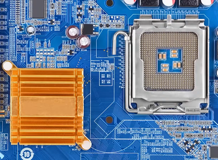
Strictly follow the spacing requirements for electronic components, ensure a safe distance between the PCB board and the housing, and follow the welding process requirements to ensure product quality and performance.
Overview
LED projector PCB assembly specifications are developed to ensure the quality and performance of LED projectors. This specification covers all aspects from PCB design, component selection, assembly process to test verification, etc., aiming to provide a complete and practical set of guiding principles.
PCB design specifications
- Layout: First, ensure that the layout of components is reasonable and meets heat dissipation requirements. Pay special attention to the layout of power supplies, LED lamp beads and thermal components.
- Routing: On the premise of meeting signal quality and power requirements, try to reduce the length and width of the traces to reduce impedance and thermal power consumption.
- Number of layers: Select the appropriate number of PCB layers according to actual needs. Consider the placement of power, signal, and ground planes to ensure proper decoupling and shielding.
- Spacing: Set the appropriate spacing between components to meet the needs of welding, maintenance and heat dissipation.
- Silk screen: clearly mark component serial numbers, models and other relevant information to facilitate identification and assembly.
Component selection specifications
- Quality: Choose brands and models with reliable quality to ensure the performance and stability of components.
- Specifications: According to actual needs, select components that meet the specifications. For example, the color temperature, brightness and other parameters of LED lamp beads must meet the design requirements.
- Temperature resistance: Considering the operating temperature of the LED projector, select components that can work stably at higher temperatures.
- Compatibility: Ensure that the selected components are compatible with the PCB design and production process.
Assembly process specifications
- Welding: Use appropriate welding methods and process parameters to ensure the quality of solder joints. Avoid false welding, false welding and other phenomena.
- Fixing: Choose the appropriate fixing method according to the component type and specifications. For example, use screws, glue, etc. to fix components.
- Insertion sequence: Assemble components according to a reasonable insertion sequence to ensure assembly efficiency and quality.
- Cleaning: Clean the PCB promptly after soldering to remove excess flux and impurities to prevent short circuits and other failures.
- Protection: During the assembly process, take necessary protective measures for sensitive components, such as applying tape, casing, etc., to prevent damage or contamination.
Test Verification Specification
- Functional test: After completing the assembly, conduct a comprehensive functional test to ensure that the functions of the LED projector are working properly.
- Performance test: Test various performance indicators of the LED projector, such as brightness, contrast, color reproduction, etc., to ensure that it meets the design requirements.
- Environmental testing: Place the LED projector under different environmental conditions (such as temperature, humidity, etc.) to test its stability and reliability.
- Life test: Test the life and reliability of the LED projector through accelerated aging tests and other methods.
- Safety test: Carry out necessary electrical safety tests, such as over-voltage, over-current protection, etc., to ensure product safety and reliability.
Quality control specifications
- Inspection: Strictly inspect each step of the process to ensure compliance with specification requirements.
- Records: Keep detailed records of all process flows and test results to facilitate traceability and analysis of problems.
- Exception handling: Deal with and record the abnormal situations discovered in a timely manner to prevent the problem from expanding or recurring.
- Continuous improvement: Based on feedback from testing and production, we continuously optimize the process and design to improve product quality and reliability.
- Training: Provide regular training to employees to improve their skill level and quality awareness to ensure the stability and reliability of product quality.
Packaging and transportation specifications
- Packaging materials: The PCB board should be packed with packaging materials such as bubble bags, pearl cotton, electrostatic bags, and vacuum bags to prevent damage during transportation.
- Anti-static packaging: Since static electricity is everywhere, especially in the dry autumn and winter seasons, static electricity may break down the chips in the PCB board, so anti-static packaging should be used during packaging and transportation.
- Moisture-proof packaging: Water vapor in the environment may penetrate into the PCB board, causing an oxidation reaction. Therefore, the PCB needs to be packed in moisture-proof packaging, and before mounting, it is best to bake it to evaporate the water vapor in the PCB to avoid the risk of board explosion caused by oxidation and welding.
- Shockproof packaging: In the packaging box, the PCB board should be placed in an anti-static packaging box, preferably placed vertically. Because a multi-layered PCB will be heavier and may be crushed. When placed vertically, no more than three layers should be stacked upward, and a stopper should be placed in the middle to maintain stability and prevent shaking.
These specifications can help protect PCB boards from damage during transportation and ensure their quality and reliability.