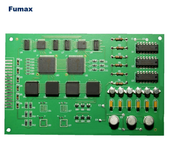
FR4 ultra-thin PCB assembly customization is an advanced electronic manufacturing technology that involves the design, manufacturing and assembly of PCB (Printed Circuit Board).
The following is a detailed introduction to FR4 ultra-thin PCB assembly customization.
Overview
FR4 is a commonly used epoxy fiberglass cloth-based material widely used in the manufacture of printed circuit boards (PCBs).
Ultra-thin PCB refers to a PCB with a thin thickness, usually between 0.2mm and 0.5mm. FR4 ultra-thin PCB has the characteristics of high density, high reliability, high thermal conductivity, etc., so it is widely used in high-end electronic products.
Design Flow
- Determine design requirements: Based on product requirements, determine PCB design requirements such as size, number of layers, wiring density, and packaging methods.
- Schematic design: Use electronic design automation (EDA) software to design circuit schematics to ensure correct circuit functions and stable performance.
- PCB layout: According to the schematic design, layout the components on the PCB to ensure that the components are arranged neatly and the wiring is reasonable.
- PCB wiring: Carry out PCB wiring design based on circuit principles and layout to ensure line conduction, impedance matching, and signal integrity.
- Design review and modification: Review the design to ensure it is correct, and make necessary modifications based on the review results.
Manufacturing process
- Plate preparation: Select the appropriate FR4 plate, cut and clean it.
- Inner layer treatment: Coating, baking and other treatments are performed on the inner layer of the board to ensure good bonding strength of the inner layer.
- Lamination: The processed inner sheets are laminated, heated and pressurized to form a multi-layer PCB.
- Drilling and hole-making: Drill holes in the PCB and plate a layer of metal conductor on the hole wall to facilitate wire connection.
- Graphic transfer: transfer circuit graphics to PCB to form conductive lines and pads, etc.
- Etching and film removal: Perform etching and film removal on the PCB to form the final circuit pattern.
- Surface treatment: Treat the surface of PCB, such as gold plating, silver plating, etc., to improve its conductivity and corrosion resistance.
- Quality inspection: Conduct quality inspection on the manufactured PCB, including appearance inspection, electrical performance testing, etc.
Assembly and customization
- Component procurement and inspection: Purchase components according to design requirements and inspect the components to ensure reliable quality.
- PCB welding: Use welding technology to weld components to PCB to achieve electrical connection between components and PCB.
- Assembly and mounting: Install other necessary components (such as capacitors, inductors, etc.) on the PCB, fix and mount them.
- Testing and debugging: Test and debug the assembled PCB to ensure its normal function and stable performance.
- Packaging and transportation: Pack and label the finished product for transportation and storage. The packaging should be shockproof and waterproof to ensure the safe transportation of the product.
- Documentation and technical support: Provide corresponding technical documentation and instructions for use, and provide follow-up technical support services as needed.
Advantages and features
- High reliability: FR4 ultra-thin PCB has the characteristics of high density and high reliability, which can ensure the long-term stable operation of the product.
- High performance: FR4 material has good thermal conductivity and electrical properties and can meet the requirements of high-performance circuits.
- Thin, light and compact: The ultra-thin design makes the product thinner, lighter and more compact, making it easy to carry and use.
- High integration: Highly integrated circuit design is achieved through high-density wiring and microvia technology.
- Customized services: We can provide personalized design, manufacturing and assembly services according to customer needs.
Application areas
- Communication equipment: FR4 ultra-thin PCB is widely used in the field of communication equipment, such as mobile phones, routers, switches, etc.
- Computer hardware: FR4 ultra-thin PCB is widely used in computer hardware, such as motherboards, graphics cards, sound cards, etc.
- Industrial control: In the field of industrial control, FR4 ultra-thin PCB is used to manufacture highly reliable control systems and equipment.
- Medical electronics: Due to its high reliability and high performance, FR4 ultra-thin PCB is also widely used in medical electronic equipment, such as monitors, medical imaging equipment, etc.
- Aerospace: In the aerospace field, due to the extremely high requirements for thinness and reliability of products, FR4 ultra-thin PCB has also been widely used.
Future trends
- 5G communication technology: With the popularization of 5G communication technology, FR4 ultra-thin PCB will usher in new development opportunities. 5G communication technology requires a large amount of high-speed signal processing and transmission, which puts forward higher requirements for PCB wiring density and signal integrity. The high performance and thinness of FR4 ultra-thin PCB will be more in line with market demand.
- Artificial Intelligence and Internet of Things: The rapid development of artificial intelligence and Internet of Things technology will further promote the application of FR4 ultra-thin PCB. Artificial intelligence and Internet of Things devices require a large amount of data processing and transmission, and require high-performance circuit boards as support, and the high integration and high reliability of FR4 ultra-thin PCB just meet this demand.
- Green and environmental protection: As society pays increasing attention to environmental protection issues, green and environmental protection has become a development trend in the electronics industry. In the future, the production and use of FR4 ultra-thin PCBs will also pay more attention to environmental protection, using more environmentally friendly materials and processes to reduce the impact on the environment.
- Personalized customization: As consumers’ demand for product personalization increases, personalized customization will become an important development direction of FR4 ultra-thin PCB. By providing personalized design, manufacturing and assembly services, we meet the needs of different customers and improve the added value and market competitiveness of our products.
To sum up, FR4 ultra-thin PCB assembly customization is a highly reliable, high-performance, lightweight and compact electronic manufacturing technology, which is widely used in communication equipment, computer hardware, industrial control, medical electronics, aerospace and other fields.
In the future, with the rapid development of 5G communication technology, artificial intelligence and the Internet of Things, green environmental protection, and personalized customization, FR4 ultra-thin PCB assembly customization technology will usher in broader development space and application prospects.