High frequency copper clad laminate technical content

High-frequency copper-clad laminates have high technical content, which is mainly reflected in the comprehensive application of special material selection, precision manufacturing technology, surface treatment technology and electrical performance testing.

The use of these technologies can ensure low loss and high stability of high-frequency signals during transmission, which is a key factor in achieving high-speed signal transmission.

The main technical content of high-frequency and high-speed copper clad laminates
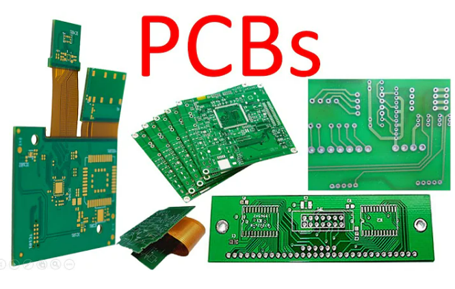
High frequency copper clad laminate technical content
  1. Material selection: High-frequency and high-speed copper-clad laminates require the use of special materials, such as resins with low dielectric constant, low loss, and high insulation performance, to ensure the stability and low loss of signal transmission. In addition, high-performance copper foil is required to improve conductivity and stability.
  2. Manufacturing process: The manufacturing process of high-frequency and high-speed copper clad laminates is relatively complex and requires multiple steps, such as copper foil processing, resin coating, hot pressing, grinding, etc. These processes require precise control to ensure the performance and stability of the final product.
  3. Surface treatment: In order to improve the electrical performance and stability of high-frequency and high-speed copper clad laminates, surface treatment is required, such as gold plating, chemical silver, etc. These processing methods require precise control to ensure the performance and stability of the final product.
  4. Testing and evaluation: High-frequency and high-speed copper-clad laminates need to undergo a series of tests and evaluations, such as dielectric constant, loss factor, heat resistance, mechanical properties, etc. These tests and evaluations require the use of professional equipment and testing methods to ensure the performance and stability of the final product.
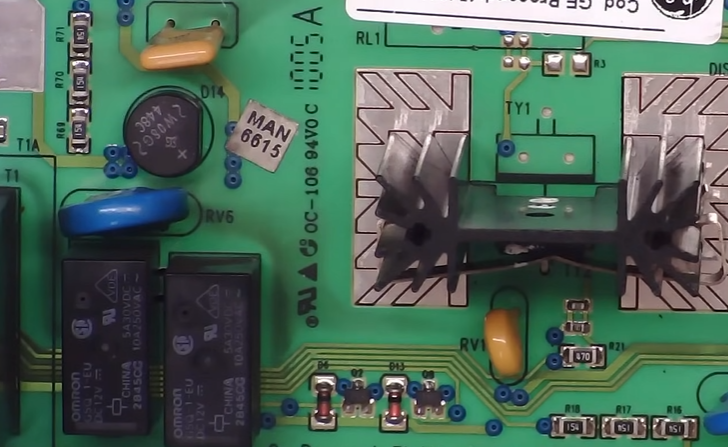
High frequency PCB factory

To sum up, high-frequency and high-speed copper-clad laminates have a high technical content and require the use of special materials and process technologies, as well as precise testing and evaluation. Therefore, only companies with higher technical level and accumulated experience can produce high-quality high-frequency and high-speed copper clad laminates.

At the same time, with the rapid development of 5G communications, Internet of Things and other fields, the application prospects of high-frequency and high-speed copper clad laminates will be broader, and market demand will continue to grow.

Frequently Asked Questions

What are the main aspects of the technical content of high-frequency copper clad laminates?

The technical content of high-frequency copper-clad laminates is mainly reflected in aspects such as material selection, manufacturing process, surface treatment, and testing and evaluation. These aspects require a high level of technology and experience accumulation to ensure the performance and stability of the final product.

Why do high-frequency copper-clad laminates need to use special materials?

High-frequency copper-clad laminates require special materials, mainly because the transmission speed of high-frequency signals is faster and the requirements for electrical performance are higher. In order to reduce the loss and interference during signal transmission, special materials such as resin with low dielectric constant, low loss, and high insulation performance need to be used to improve the signal transmission quality and stability.

What are the characteristics of the manufacturing process of high-frequency copper clad laminates?

The manufacturing process of high-frequency copper-clad laminates is relatively complex and requires precise control. Common manufacturing processes include copper foil processing, resin coating, hot pressing, grinding, etc. These processes need to be selected and optimized based on specific materials and requirements to ensure the performance and stability of the final product.

What are the surface treatment methods for high frequency copper clad laminates?

Surface treatment methods for high-frequency copper-clad laminates include gold plating, chemical silver, etc. These processing methods can improve the electrical performance and stability of the product, but also require precise control to ensure the performance and quality of the final product.

What testing and evaluation are required for high frequency copper clad laminates?

High-frequency copper-clad laminates require a series of tests and evaluations, including dielectric constant, loss factor, heat resistance, mechanical properties, etc. These tests and evaluations require the use of professional equipment and testing methods to ensure the performance and stability of the final product.

What is the market prospect of high-frequency copper clad laminates?

With the rapid development of 5G communications, Internet of Things and other fields, the market prospects of high-frequency copper clad laminates are very broad. In the future, with the continuous advancement of technology and the increase in application demand, the market demand for high-frequency copper clad laminates will also continue to grow.

Related Posts

HDI PCB’s Advantages in Industrial electronics

Why HDI and how does it work In the realm of industrial control systems, High-Density Interconnect (HDI) Printed Circuit Boards (PCBs) have emerged as transformative components, revolutionizing the landscape of modern manufacturing and automation. HDI PCBs play a pivotal role in enhancing the functionality, reliability, and compactness of various industrial devices, facilitating an era of […]

Introduction to IPC Standards in PCB Manufacturing and Assembly

The IPC (Association Connecting Electronics Industries) is a global trade association that develops standards for the electronics manufacturing industry. These standards are crucial for ensuring quality, reliability, and consistency in the production of printed circuit boards (PCBs) and their assembly. This article will cover the main IPC standards relevant to PCB manufacturing and assembly, detail […]

Solder Paste, Rosin, and Flux: Differences and Which One to Use?

Why Rosin and Flux Help with Soldering Rosin and flux make soldering easier for a few key reasons: How They Work Rosin: When heated, it decomposes into active components that remove oxides and form a protective gas to prevent further oxidation. Flux: Contains various active ingredients that become active at high temperatures, cleaning oxides, improving […]

How to design PCB for IoT Products with UWB Modules

Designing PCBs for Internet of Things (IoT) products, especially those incorporating Ultra-Wideband (UWB) modules, involves a unique set of challenges and considerations. These include ensuring optimal electrical performance, thermal management, mechanical strength, manufacturability, environmental compliance, and cost-effectiveness. This article delves into the specific factors engineers need to consider when designing PCBs for IoT products with […]

Understanding Motors: Types, Control PCB Design, and Top 10 Chinese Manufacturers

What are Motors and Their Types? Motors are essential devices that convert electrical energy into mechanical energy, powering countless applications from household appliances to industrial machinery. Understanding the different types of motors is crucial for selecting the right one for your needs. Here are the main types of motors: Designing and Producing Motor Control PCBs […]

Multi-layer PCB Assembly Guideline in 2024

Multi-layer PCBs (Printed Circuit Boards) are widely used in modern electronic devices due to their capability to provide more routing layers, higher electrical performance, and reduced size. However, assembling multi-layer PCBs involves several critical steps and meticulous attention to detail to ensure the final product’s quality and reliability. Below are the detailed considerations to keep […]

Introduction to PCBA Testing Jigs

In the electronics manufacturing industry, ensuring the quality and functionality of Printed Circuit Board Assemblies (PCBAs) is crucial. One of the key tools used in this process is the PCBA testing jig. This article will provide an in-depth overview of what a PCBA testing jig is, its basic structure, how it is manufactured, and how […]

Unveiling Circuit Card Assembly 2024: From PCB Manufacturing to Board Assembly

Hey there, tech enthusiasts! Get ready to dive deep into the fascinating world of circuit card assembly. In this comprehensive guide, we’ll take you through every meticulous step of the process, from PCB manufacturing to the final assembly of the board. So grab your coffee, settle in, and let’s explore the intricate journey of bringing […]

Optimizing High-Speed Design: Balancing Signal, Power, and EMC for Success

Editor’s Note: In modern high-speed designs, analyzing signal integrity, power integrity, and EMC separately is not enough; a holistic approach is essential for successful design. Background Issue: When signals cross over segmentation areas between adjacent reference planes on a layer, discussions about signal integrity often arise. Some argue that signals should not cross the segmentation […]