Thermoelectric separation copper substrate processing flow and technical points?

Thermoelectric separation of copper substrate refers to a thermoelectric separation process in copper substrate processing.

The circuit part of the substrate and the thermal layer part are on different circuit layers.

The thermal layer part is in direct contact with the heat dissipation part of the lamp bead to achieve the best heat dissipation and heat conduction effect. .

The thermal conductivity of the thermoelectric separation copper substrate is 398W/M.K, which overcomes the shortcomings of insufficient heat conduction and heat dissipation of existing copper substrates.

This process conducts the heat generated by electronic components directly through the heat dissipation area, greatly improving the heat dissipation effect.
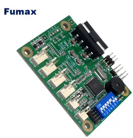
Thermoelectric separation copper substrate processing flow and technical points?

The thermoelectric separation copper substrate can separate the thermal layer and the circuit layer through the following process flow, so that the heat generated by the components can be directly conducted through the heat dissipation area, and the thermal conductivity efficiency is greatly improved, thus increasing the service life of the product.

Thermoelectric separation copper substrate processing flow and technical points

  1. BOARD CUT, the purpose is to cut the substrate material into the size required for the work according to the planning requirements of the pre-production design.
  2. Baking plate: FR-4/BT materials need to be baked before production.
  3. Panel production.
  4. Exposure (EXPOSURE), the graphics on the original film are transferred to the photosensitive plate through the action of light.
  5. Develop (DEVELOPING), use developer (sodium carbonate) to decompose the unnecessary part of the wet film, and save the necessary part.
  6. Etching (ETCHING), using etching solution (alkaline copper chloride) to etch away the surface copper exposed after development to form a wiring pattern.
  7. Panel cleaning, panel cleaning and drying. After the panel is etched, fill the plastic frame with water and soak it for cleaning. After passing through the water, place it on a horizontal line and bake it in the back section (such as a plate washer, film stripping line, plate grinder, etc.) .
  8. Apply AD glue, target, and brown.
  9. Rotate the panel so that the boss matches the joint between the panel and the panel.
  10. Target shooting again, remove the film and target again, select 4 points again to add foolproofing.
  11. The grinding plate is soldered, coated with ordinary oil through the tunnel furnace, and artificially printed with miscellaneous oil (such as WG91, WT32, black sun oil, etc.).
  12. Expose solder mask and print characters.
  13. Forming and drilling. After forming and drilling, tear off the green film on the back and cut in V.
  14. Pass through the wire drawing machine, and pass the single panel V through the wire drawing machine to refine the back cloak.
  15. For anti-oxidation treatment, OSP boards are sent to peroxidation, tin-sprayed boards are sent to the board washing room, and immersion gold boards are sent to the board washing room.
  16. Pack and ship, place orders for shipment, and do not omit any reports that should be attached according to the process card.

The formation process of thermoelectric separation copper substrate includes sticking protective tape on one side of the copper base layer; forming anti-etching ink, exposure, development and etching through the circuit board process to form bumps in the heat dissipation area, and the height of the bumps is equal to the thickness of the insulation layer and circuit layer ; A layer of copper plating is electroplated on the aluminum surface through zinc immersion and copper electroplating processes; the circuit layer (copper foil) and the insulation layer (non-flowing prepreg) are stacked together.

Open a window in the heat dissipation area of the circuit layer and insulation layer. You can use die cutting or CNC molding to open the window; combine the heat dissipation layer (copper-plated aluminum substrate) with the circuit layer (copper foil) and insulation layer (non-flowing epoxy The prepregs) are pressed together by hot pressing; the circuit layer lines are produced according to the circuit board processing process to form the thermoelectric separation metal substrate provided by the present utility model.

Related Posts

HDI PCB’s Advantages in Industrial electronics

Why HDI and how does it work In the realm of industrial control systems, High-Density Interconnect (HDI) Printed Circuit Boards (PCBs) have emerged as transformative components, revolutionizing the landscape of modern manufacturing and automation. HDI PCBs play a pivotal role in enhancing the functionality, reliability, and compactness of various industrial devices, facilitating an era of […]

Introduction to IPC Standards in PCB Manufacturing and Assembly

The IPC (Association Connecting Electronics Industries) is a global trade association that develops standards for the electronics manufacturing industry. These standards are crucial for ensuring quality, reliability, and consistency in the production of printed circuit boards (PCBs) and their assembly. This article will cover the main IPC standards relevant to PCB manufacturing and assembly, detail […]

Solder Paste, Rosin, and Flux: Differences and Which One to Use?

Why Rosin and Flux Help with Soldering Rosin and flux make soldering easier for a few key reasons: How They Work Rosin: When heated, it decomposes into active components that remove oxides and form a protective gas to prevent further oxidation. Flux: Contains various active ingredients that become active at high temperatures, cleaning oxides, improving […]

How to design PCB for IoT Products with UWB Modules

Designing PCBs for Internet of Things (IoT) products, especially those incorporating Ultra-Wideband (UWB) modules, involves a unique set of challenges and considerations. These include ensuring optimal electrical performance, thermal management, mechanical strength, manufacturability, environmental compliance, and cost-effectiveness. This article delves into the specific factors engineers need to consider when designing PCBs for IoT products with […]

Understanding Motors: Types, Control PCB Design, and Top 10 Chinese Manufacturers

What are Motors and Their Types? Motors are essential devices that convert electrical energy into mechanical energy, powering countless applications from household appliances to industrial machinery. Understanding the different types of motors is crucial for selecting the right one for your needs. Here are the main types of motors: Designing and Producing Motor Control PCBs […]

Multi-layer PCB Assembly Guideline in 2024

Multi-layer PCBs (Printed Circuit Boards) are widely used in modern electronic devices due to their capability to provide more routing layers, higher electrical performance, and reduced size. However, assembling multi-layer PCBs involves several critical steps and meticulous attention to detail to ensure the final product’s quality and reliability. Below are the detailed considerations to keep […]

Introduction to PCBA Testing Jigs

In the electronics manufacturing industry, ensuring the quality and functionality of Printed Circuit Board Assemblies (PCBAs) is crucial. One of the key tools used in this process is the PCBA testing jig. This article will provide an in-depth overview of what a PCBA testing jig is, its basic structure, how it is manufactured, and how […]

Unveiling Circuit Card Assembly 2024: From PCB Manufacturing to Board Assembly

Hey there, tech enthusiasts! Get ready to dive deep into the fascinating world of circuit card assembly. In this comprehensive guide, we’ll take you through every meticulous step of the process, from PCB manufacturing to the final assembly of the board. So grab your coffee, settle in, and let’s explore the intricate journey of bringing […]

Optimizing High-Speed Design: Balancing Signal, Power, and EMC for Success

Editor’s Note: In modern high-speed designs, analyzing signal integrity, power integrity, and EMC separately is not enough; a holistic approach is essential for successful design. Background Issue: When signals cross over segmentation areas between adjacent reference planes on a layer, discussions about signal integrity often arise. Some argue that signals should not cross the segmentation […]