Radio Frequency (RF) PCB board assembly and circuit wiring is a complex process involving multiple considerations.
The following is a detailed introduction to this topic, divided into two parts: assembly and wiring.
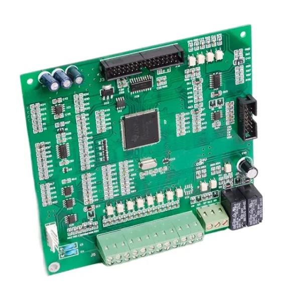
RF PCB board assembly
When assembling an RF PCB board, certain rules and best practices need to be followed to ensure signal integrity and system stability.
Here are the key steps and considerations:
- Component selection: Choosing the right components is critical to RF performance. Components must have low inductance, low capacitance, and low loss to reduce signal loss and interference. Additionally, the physical dimensions and pin spacing of the components need to be considered to ensure they fit onto the pads on the PCB board.
- Pad design: The pad is the connection point between the component and the PCB board and must be carefully designed to ensure a reliable connection. The pad size should be appropriate for easy soldering and good electrical contact. In addition, the matching between component pin spacing and pad spacing should also be considered.
- Layout: In terms of layout, sensitive RF components need to be placed close to the center to reduce signal path length and interference. Additionally, optimal power and grounding strategies should be followed to ensure a stable power supply and effective grounding. Traces between components should be as short, straight, and wide as possible to reduce resistance and inductance in the signal path.
- Assembly process: During the assembly process, appropriate soldering techniques, such as hot air soldering or reflow soldering, should be used to ensure reliable connections between components and PCB boards. Additionally, clean and consistent soldering practices should be followed to reduce failures or performance issues due to poor soldering.
- Testing and verification: After completion of assembly, comprehensive testing and verification should be performed to ensure that performance meets requirements. This includes testing key parameters, checking signal quality and spectrum performance, and troubleshooting.
RF circuit wiring
RF circuit wiring is a key link to ensure signal quality and system stability. Here are some key best practices:
- Line width and line spacing: Line width and line spacing should be selected based on the required signal frequency, impedance matching and maximum voltage drop. Wider line widths reduce resistance and increase current handling, while smaller line spacing reduces capacitive coupling and improves signal isolation.
- Wiring direction: Where possible, the wiring direction should be consistent to reduce signal path length and wiring discontinuities. In addition, vertical wiring can reduce the length of parallel wiring, thereby reducing electromagnetic interference (EMI).
- Grounding strategy: A correct grounding strategy is crucial to the quality of RF signals. The ground plane should be placed as close as possible to the wiring layer to reduce the inductance of the signal return path. In addition, multiple ground planes can help improve the electromagnetic compatibility (EMC) of the system.
- Shielding: For sensitive RF signals, metal shielding cavities or other shielding measures can be used to reduce the impact of EMI and other interference sources. Shielding can significantly improve signal quality and reduce error rates.
- Corners and branches: During wiring, sudden corners and branches should be avoided as they may cause signal discontinuities and reflections. Where corners are required, 45-degree angles or arc-shaped corners should be used to reduce signal loss and reflections.
- Termination method: For RF signals, it is very important to use appropriate termination method. Common termination methods include series terminals, parallel terminals, and Thevenin terminals. The most appropriate termination method should be selected based on specific application requirements.
- Wiring materials: Wiring materials have a great impact on the quality of RF signals. Choosing materials with low inductance and low losses is critical to reducing signal loss. Common wiring materials include metallic conductors such as copper, gold, and silver, and insulating materials such as polyimide and polytetrafluoroethylene.
- Simulation and optimization: When performing RF wiring, it is very important to use simulation software for signal integrity analysis. This helps uncover potential signal discontinuities and reflection issues and guides designers to make necessary optimization changes. Through the optimization function of the simulation software, the performance and reliability of the RF circuit can be further improved.
- Verification and testing: After wiring is completed, comprehensive verification and testing should be performed to ensure that performance meets requirements. This includes steps such as testing key parameters, checking signal quality and spectrum performance, and troubleshooting. The quality and reliability of RF circuit wiring can be ensured through a rigorous testing and verification process.
In summary, RF PCB board assembly and circuit routing need to follow a series of best practices to ensure signal integrity and system stability.
From component selection to simulation and optimization, every step is critical. Through careful design and strict quality control, high-performance, reliable RF circuit boards can be created, thereby improving overall system performance.