Methods for PCB pad surface treatment are used to protect the PCB pads and improve soldering performance.
- ENIG
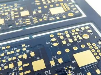
ENIG (Electroless Nickel Immersion Gold) and immersion gold plating are commonly used processes in today’s PCB production. With the increasing integration of ICs and the growing number of pins, vertical tin spraying processes struggle to flatten small pads, posing challenges for SMT assembly. Additionally, the shelf life of tin-sprayed boards is short. ENIG or immersion gold plating addresses these issues effectively.
For surface mount technology, especially for ultra-small components like 0603 and 0402, pad flatness directly impacts solder paste printing quality, which crucially affects subsequent reflow soldering quality. Therefore, whole board ENIG or immersion gold plating is frequently seen in high-density and ultra-small component surface mount processes.
During the prototyping phase, due to factors like component procurement, boards often sit idle for weeks or even months before use. The shelf life of ENIG or immersion gold-plated boards is much longer compared to tin-plated ones, making them preferable. Moreover, the cost of ENIG or immersion gold PCBs during the sampling phase is comparable to that of lead-tin alloy boards.
ENIG involves coating the pads with a layer of electroless nickel as an intermediate layer, followed by a layer of gold on the nickel surface. ENIG offers benefits such as good wettability, flatness, corrosion resistance, and excellent solderability. Additionally, gold’s properties aid in preventing oxidation, thus enhancing long-term storage stability.
- HASL:
Hot Air Solder Leveling (HASL) is another common surface treatment method. During the HASL process, the pads are immersed in a pot of molten tin alloy, and excess tin is blown away by hot air, leaving behind a uniform tin layer. The advantages of HASL include lower cost, ease of manufacturing, and soldering. However, relative to other methods, its surface accuracy and flatness may be lower.
- Gold Plating
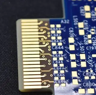
Gold plating is a method of depositing a layer of gold onto PCB pads. Gold exhibits excellent electrical conductivity and corrosion resistance, which enhances soldering quality. However, compared to other methods, gold plating typically incurs higher costs. It is particularly applied in surface treatments for gold fingers.
- IAG:
Immersion Silver (IAg) jazzes up PCBs by chemically displacing it directly onto the base metal. It’s like the more affordable cousin of ENIG, plus it’s totally RoHS-compliant. Think of it as a fashionista with a typical thickness ranging from 4 to 12u”. And here’s a fun fact: because copper and silver are like BFFs, they eventually meld into one another.
Why it rocks: Gives you a flat, smooth surface to work your soldering magic on, totally lead-free and RoHS compliant, and holds tighter tolerances for those plated holes. Plus, it’s the go-to for low loss in signal integrity applications.
What’s not so hot: Handling the PCB can stir up some soldering trouble, it’s more bang for your buck compared to ENIG but not as thrifty as Immersion Tin. And beware, the finish can get a bit tarnished and oxidized over time.
- IMMERSION TIN
Immersion Tin (ISn) jazzes up PCBs by chemically displacing it directly onto the base metal. It’s like the thriftier sibling of ENIG and Immersion Silver, and guess what? It’s totally RoHS-compliant too. Picture it with a typical thickness ranging from 20 to 50u”. And here’s a fun tidbit: because tin and copper are like two peas in a pod, they eventually meld into one another.
Why it’s rad: Gives you a flat, smooth surface to work your soldering magic on, totally lead-free and RoHS compliant, and holds tighter tolerances for those plated holes. It’s also the go-to for press fit applications, making it a hit among PCB enthusiasts.
What’s not so cool: Handling the PCB can be a bit risky, potentially leading to damage and soldering woes. Watch out for tin whiskers too, and remember, its shelf life is shorter compared to ENIG.
- OSP
Organic Solderability Preservatives, is a popular surface treatment method for PCBs. It’s a hot topic in the PCB industry, and recent articles have shed light on its benefits and applications.
OSP works by applying a thin organic layer to the copper pads of a PCB, protecting them from oxidation and ensuring excellent solderability. This method is gaining traction due to its eco-friendly nature and cost-effectiveness compared to traditional treatments like HASL and ENIG.
Recent articles have highlighted OSP’s advantages, such as its ability to provide a flat surface for soldering, its lead-free and RoHS compliance, and its suitability for fine-pitch components. Additionally, OSP offers improved thermal reliability and better performance in high-frequency applications.
However, it’s essential to consider some challenges associated with OSP, such as its sensitivity to handling, potential shelf life issues, and compatibility with certain assembly processes.
Overall, OSP is an exciting innovation in PCB surface treatment, and the recent articles provide valuable insights into its use and potential in modern electronics manufacturing.
- HARD GOLD
When it comes to PCB surface finishes, hard gold stands out as one of the priciest options, but boy, does it pack a punch! Hard gold applications are like the superheroes of durability, boasting a shelf life that’s longer than your favorite book series. We’re talking about thickness rates that range from 30 μin gold over 100 μin nickel to 50 μin gold over 100 μin nickel, making them tough as nails.
But wait, there’s more! Hard gold isn’t just for show; it’s reserved for components that are in it for the long haul. Think edge connectors, battery contacts, and those special test boards that never seem to take a break.
Advantages? You bet! With hard gold, you get a surface that laughs in the face of wear and tear, plus it’s lead-free and totally RoHS compliant. Oh, and did I mention the shelf life? It’s so long, you’ll forget you even ordered it.
Now, onto the downsides: Hard gold is like that luxury sports car of surface finishes – it’s expensive. And sometimes, you might need to throw in some bus plating and a little extra elbow grease during assembly. But hey, when you’re aiming for the best, a little extra effort is totally worth it, right?
In conclusion, the selection of PCB surface treatment involves weighing the trade-offs between cost, performance, and environmental impact. Understanding the unique characteristics of each method enables manufacturers to make informed decisions based on the specific needs of their projects.