PCB LCD design and assembly is one of the core technologies for manufacturing electronic equipment, involving circuit board design and manufacturing, electronic component assembly, display integration and other aspects.
- What are the manufacturing methods of LCD screen IC?
- An assembly structure of LCD panel and PCB board
- Function expansion of PCB in LCD module
- About PCB board optimization design for LCD electrical testing
- A PCB board backing tool for LCD display assembly
- PCB LCD design and assembly process technology
- PCB LCD design and assembly process technology
- LCD TV assembly factory
What are the manufacturing methods of LCD screen IC?
The following are several common manufacturing methods of LCD screen ICs:
- COG (Chip on Glass) method: the chip is directly pasted on the glass substrate, suitable for small-sized LCD screens.
- COF (Chip on Flex) method: the chip is directly pasted on the flexible substrate, suitable for larger size LCD screens.
- TCP/CTP (Tape Carrier Package/Chip on Tape Package) method: The chip is packaged on a film carrier and then pasted on a glass substrate or flexible substrate, suitable for large-size LCD screens.
- COB (Chip on Board) method: Paste the chip directly on the circuit board, suitable for small-size LCD screens.
Each of these manufacturing methods has advantages and disadvantages, and the appropriate manufacturing method should be selected based on specific application requirements.
An assembly structure of LCD panel and PCB board
An assembly structure of an LCD panel and a PCB board, including the connection between the LCD panel and the PCB board through metal bent pins. The metal bent pins include lower pins and two upper tube corners. The two tube corners are installed symmetrically up and down. On the upper part of the tube pin, a tube corner groove is formed between the two tube corners. Both ends of the LCD panel are inserted into the tube corner groove, and the bottom part of the tube foot is inserted into the hole of the PCB board. This structure uses metal bent pins to buffer and relieve stress, completely solving undesirable problems such as product edge discoloration and product fragmentation, and improving product reliability.
Function expansion of PCB in LCD module
In LCD modules, the functional expansion of PCB (Printed Circuit Board) mainly includes the following aspects:
- Multi-interface merger: For an LCD module with touch function, it will have multiple interfaces. By merging multiple interfaces, such as those for LCD and CTP, the location of one connector can be saved, which is an effective solution for applications with compact motherboards. At the same time, this merger also makes assembly easier.
- Signal conversion: When the interface of the mainstream LCD screen on the market does not match the motherboard solution, a signal conversion solution can be used. For example, convert the RGB interface to an MCU interface to meet usage needs.
- PCB positioning posts: In order to meet the seismic requirements of some LCD modules, in addition to using double-sided tape, screw holes can also be used for fixation. When designing the PCB, you can increase the size of the PCB on the outside of the LCM and add openings on it to accommodate different screws.
In addition, with the continuous improvement of the integration and assembly density of electronic components, and the miniaturization and ultra-miniaturization of electronic components, PCB boards are not only suitable for single-layer and double-sided boards, but are also widely used in multi-layer boards with high wiring density. These multilayer boards may reach 68 layers and 4 layers in LCD liquid crystal modules. At the same time, in order to adapt to the development of fine pitch and multi-lead technology for surface mount components, the wiring density of PCBs is gradually increasing. Compared with traditional plug-in printed boards, the area of surface-mounted printed boards is reduced by 60%, the weight is reduced by 80%, and the circuit logic density is increased by more than 5 times.
About PCB board optimization design for LCD electrical testing
The optimal design of PCB boards for LCD electrical testing needs to take into account many factors. Here are some suggestions:
- Select the appropriate substrate: Select the appropriate substrate according to the actual application requirements. For example, in high temperature, high humidity, and highly corrosive environments, substrates with high temperature resistance and corrosion resistance should be selected.
- Optimize circuit design: In order to improve the signal quality and anti-interference ability of the PCB board, it is necessary to optimize the circuit design. For example, when wiring, the length and bending of the lines should be minimized, and parallel routing should be avoided to reduce interference between signals. In addition, ground wires should be placed around key signal lines to reduce electromagnetic interference.
- Add power and ground layers: In order to improve the stability of power and ground, you can add power and ground layers on the PCB board. This can not only improve the anti-interference ability of the power supply and ground wires, but also reduce the voltage drop on the power supply and ground wires.
- Optimize component layout: The reasonableness of component layout directly affects the signal quality and anti-interference ability of the PCB board. Therefore, when laying out components, the distance and height difference between components should be minimized, and sensitive components should be avoided to be placed close to interference sources.
- Set appropriate via holes: The setting of via holes is also an important factor affecting the performance of the PCB board. If too many vias are provided, the thickness of the PCB board will increase and the interference between signals will also increase. Therefore, when setting via holes, the number and diameter of via holes should be reduced as much as possible, and at the same time, avoid setting via holes near signal lines.
- Consider thermal design: LCDs operating in high temperature environments need to consider thermal design. In order to improve the heat dissipation effect, you can set a heat sink on the PCB board or use materials with good thermal conductivity to make the PCB board.
- Consider maintainability: In order to facilitate the maintenance and replacement of components, a maintenance window can be set on the PCB board or a modular design can be adopted to facilitate the replacement of components without affecting the work of other parts.
In short, the optimal design of PCB boards for LCD electrical testing needs to take into account various factors, including substrate selection, circuit design, power and ground layer settings, component layout, via settings, thermal design and maintainability. Only by comprehensively considering these factors can a PCB board for LCD electrical testing with excellent performance be designed.
A PCB board backing tool for LCD display assembly
The following is a PCB board backing tool for LCD display assembly:
The tooling includes tooling base and split back support. The upper surface of the tooling base is provided with a plurality of positioning pins, and the lower surface of the split back support is provided with positioning holes corresponding to the number and position of the positioning pins. This design allows the PCB board to be accurately fixed on the back support while being easy to remove and replace.
In addition, the upper surface of the split back support is also provided with positioning blocks to limit the movement of the PCB board along the Y-axis direction. The number and position of the positioning blocks correspond to the number and position of the positioning holes on the split back support. This design can ensure the stability and accuracy of the PCB board during assembly.
The tooling base is also equipped with positioning stops to limit the movement of the PCB board along the X-axis direction. The number and position of the positioning stops correspond to the number and position of the positioning holes on the split back support. This design can further enhance the stability of the PCB board during assembly.
Finally, the tooling also includes several locking screws. These screws are used to lock the split back support and the tooling base to ensure the stability and accuracy of the PCB board during assembly.
In short, this kind of PCB board backing tooling for LCD display assembly has reasonable design, easy use, high precision and good stability, and is suitable for mass production.
PCB LCD design and assembly process technology
The assembly process of LCD TV includes the following steps:
- Prepare tools and raw materials: including LCD screen, PCB board, power supply, shell, screws, etc.
- Install the shell: Place the shell correctly on the workbench according to the instructions on the process card. Pay attention to the correct direction of the shell.
- Install the LCD screen: Place the LCD screen correctly into the case according to the instructions on the process card.
- Connect the circuit: Align the circuit board to the frame position according to the instructions on the process card, install it into the shell and press it tightly, and use special assembly tools to fix the shell and circuit board.
- Install the backlight: If you need to add a backlight, fix the backlight on the PCB first.
- Wiring: Network cables are generally used as control lines between splicing screens. Each screen is connected in series with network cables. The network cables of the screens must be connected to the serial port on the computer, so that the entire large screen can be controlled.
- Debugging: After the screen is powered on, the screen can be debugged. Each screen displays an address code through the computer serial port, assigns the location of the screen, and sends commands to it. The screen debugging is completed.
- Testing: Assembled products need to be tested and can enter the market only after passing the test.
The above is the basic process of LCD TV assembly. The specific processes of different companies may be slightly different.
PCB LCD design and assembly process technology
PCB LCD design and assembly process technology mainly includes the following steps:
- Design: First, you need to design the PCB according to the circuit schematic diagram. Various factors need to be considered during the design process, such as the layout of external connections, optimized layout of internal electronic components, optimized layout of metal connections and through holes, electromagnetic protection, heat dissipation, etc. Excellent layout design can save production costs and achieve good circuit performance and heat dissipation performance. Simple layout design can be realized by hand, while complex layout design requires computer-aided design (CAD).
- Manufacturing: During the PCB manufacturing process, it is necessary to ensure the matching of the substrate and components, and at the same time control the production cost. The manufacturing process includes multiple steps such as etching, drilling, plating, welding, etc.
- Assembly: Assemble the PCB with other components such as LCD display, power supply, control board, etc. to form a complete LCD display. Certain process flows and standards need to be followed during the assembly process to ensure product quality and stability.
- Testing: After assembly is completed, the product needs to be tested to ensure that its performance and quality meet the requirements. Testing includes many aspects, such as appearance testing, functional testing, performance testing, etc.
PCB LCD design and assembly process technology requires multiple links and steps, and each link requires strict quality control and process standards to ensure product quality and stability. At the same time, with the continuous advancement of technology and changing application requirements, these technologies and standards are constantly being updated and improved.
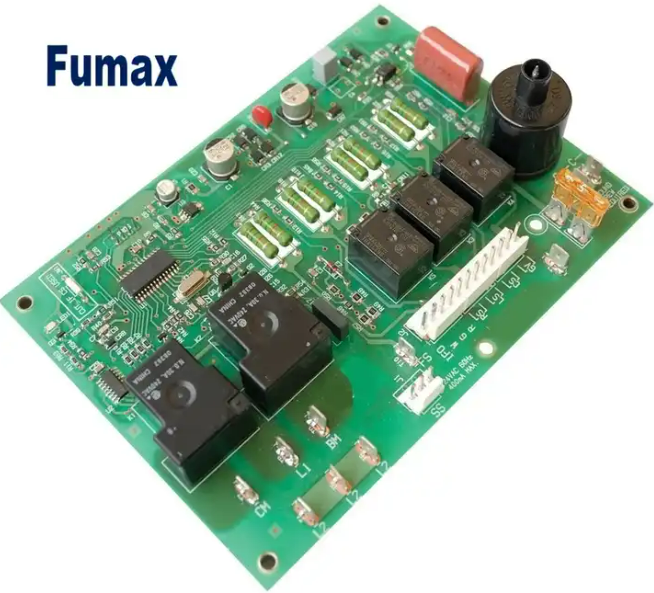
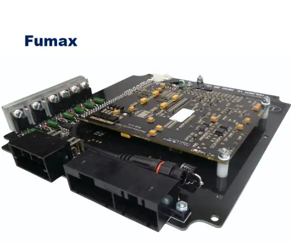
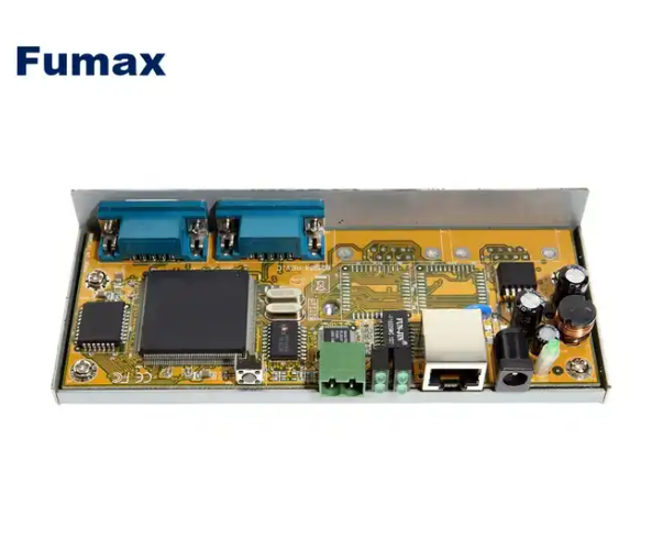
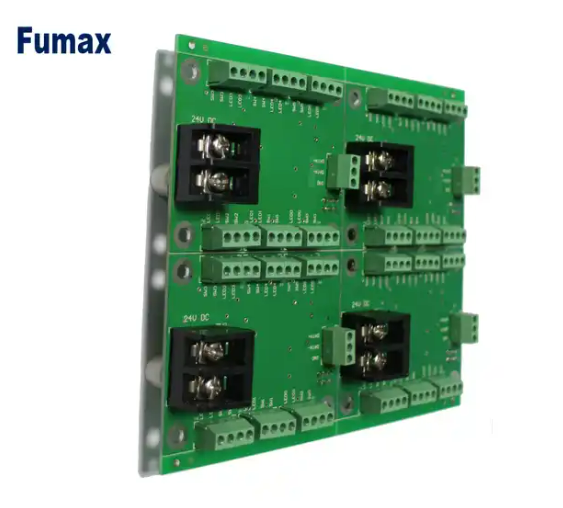
LCD TV assembly factory
Fumax factory provides LCD display PCB circuit board manufacturing, PCB assembly, and PCBA customization services. Fumax is your one-stop OEM/ODM PCB assembly factory.