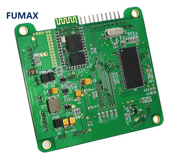
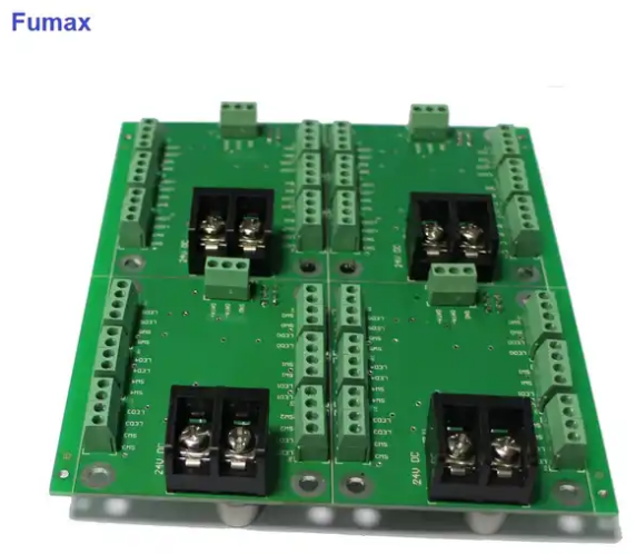
What is a power tool control panel
The power tool control panel is a device used to control power tools. It can realize functions such as starting, stopping, and speed adjustment of power tools.
- What is a power tool control panel
- What is PCB power tool control board design
- PCB power tool control board design process
- What software is needed in the design process of PCB power tool control board?
- What should we pay attention to when designing PCB power tool control board?
- What material is used for PCB power tool control board?
- Why does PCB power tool control board use rigid substrate material?
- What documents do I need to provide to the manufacturer for power tool control panel PCB customization?
- How does the power tool control panel manufacturing process work?
- Contact information of PCB power tool control board design manufacturer
What is PCB power tool control board design
PCB power tool control board design refers to the use of electronic design automation (EDA) software to design the circuit board and design the layout and circuit connections of the printed circuit board (PCB) to meet the performance and reliability requirements of the power tool. In the design of the power tool control board PCB, factors such as circuit layout, routing, component selection and placement, and separation of power supply and signals need to be considered to ensure the stability and reliability of the circuit. At the same time, the functional requirements and electromagnetic compatibility requirements of the circuit also need to be met. After the design is completed, testing and debugging are also required to ensure that the function and performance of the control board meet the design requirements.
PCB power tool control board design process
The design process of a power tool control panel usually includes the following steps:
- Determine control requirements: Based on the specific application scenarios and functional requirements of the power tool, determine the functions and control methods that the control panel needs to implement.
- Select the appropriate microcontroller: According to the control needs and performance requirements, select the appropriate microcontroller as the core component of the control board.
- Design the circuit board: Design the structure and layout of the circuit board based on the pin assignment and circuit design of the microcontroller.
- Select the required electronic components: According to the needs of the circuit design, select the required electronic components, such as power supply, resistor, capacitor, diode, transistor, etc.
- Make PCB: Make PCB circuit board according to the design and component selection of the circuit board.
- Testing and debugging: After the production is completed, the control board is tested and debugged to ensure that its functions and performance meet the design requirements.
In the process of designing power tool control boards, it is usually necessary to use EDA software, such as Altium Designer, Eagle, etc., for circuit design and PCB production.
What software is needed in the design process of PCB power tool control board?
In the PCB power tool control board design process, commonly used EDA software includes Altium Designer, Eagle, CAD, etc. These softwares all have functions such as circuit board design, component library management, and circuit simulation, which can meet the design needs of power tool control boards.
Among them, Altium Designer software has the characteristics of simple operation, powerful functions, easy to learn and use, etc., and is widely used in the field of electronic design. When choosing EDA software, you need to choose based on personal needs and actual conditions, and be familiar with the operation and design specifications of the software.
What should we pay attention to when designing PCB power tool control board?
When designing PCB power tool control boards, you need to pay attention to the following points:
- Select the appropriate PCB material: According to the application scenario and component requirements, select the appropriate PCB material, such as FR4, CEM-1, etc.
- Consider the thickness and size of the PCB: Choose the appropriate PCB thickness and size based on the application scenario and component layout.
- Optimize the PCB layout: Based on the circuit design and component layout, optimize the PCB layout to ensure that the PCB structure is reasonable, beautiful, and easy to maintain.
- Pay attention to the wiring rules of the PCB: According to the circuit design and component requirements, pay attention to the wiring rules of the PCB to ensure the stability and reliability of the signal.
- Thicken the power cord and ground wire: In order to improve the stability of the power supply and signal, it is necessary to thicken the diameter of the power cord and ground wire.
What material is used for PCB power tool control board?
Power tool control board PCB usually uses copper-clad laminate as the substrate material. Common ones are FR-4 (glass fiber cloth soaked with epoxy resin) and CEM-1 (glass fiber cloth soaked with acrylonitrile-butylphenol-styrene copolymer). wait.
These materials have high mechanical strength, electrical properties and heat resistance, and can meet the complex circuit design and high reliability requirements of power tool control boards. When selecting PCB materials, you need to choose based on design requirements and application scenarios, and consider factors such as material reliability, cost, and processing difficulty.
Why does PCB power tool control board use rigid substrate material?
The general rigid substrate material is copper-clad laminate, which is made of reinforcing material, soaked in resin adhesive, dried, cut, and laminated into a blank, then covered with copper foil, using a steel plate as a mold, and then pressed in a hot press It is made by high temperature and high pressure forming processing.
What documents do I need to provide to the manufacturer for power tool control panel PCB customization?
When customizing the power tool control board PCB, the following documents need to be provided to the manufacturer:
- PCB design files: including circuit diagram, PCB diagram, BOM list, etc.
- Component list: includes information such as model, specification, quantity and so on of all electronic components.
- Design specification: including design requirements, functional description, performance parameters and other information.
- Other related documents: such as production orders, quality control documents, etc.
How does the power tool control panel manufacturing process work?
The manufacturing process of power tool control panels usually includes the following steps:
- Material preparation: Prepare the required electronic components and PCB materials based on the design documents and component list.
- SMT: Mount the electronic components on the PCB according to the requirements of the design document.
- Welding: Weld the mounted PCB and connect various electronic components.
- Testing: After welding is completed, test and debug the control board to ensure that its functions and performance meet the design requirements.
- Assembly: Assemble the tested PCB with other mechanical components to form a complete power tool control board.
- Inspection: Conduct quality inspection on the assembled power tool control board to ensure that it meets production standards and customer requirements.
- Shipping: Pack and ship the qualified power tool control boards.
Contact information of PCB power tool control board design manufacturer
There are many PCBB design, PCB manufacturing, and PCB assembly factories in China. The following recommended PCB power tool control board design manufacturers in Shenzhen, China, have contact information as follows:
Full company name: Shenzhen Fumax Technology Co., Ltd.
Company address: Room 2705, East Building, Yihai Building, Chuangye Road, Nanshan District, Shenzhen, China.
PCB Factory address: 5th Floor, Building 4, Huafeng Science and Technology Park, Fengtang Avenue, Tangwei Community, Fuhai Street, Baoan District, Shenzhen City
Contact information: PCB power tool control board design and customization factory contact information.