PCB BGA packaging is a high-density, small-volume integrated circuit packaging form. It uses ball grid array (BGA) as the packaging form. It has the advantages of high reliability and high electrical performance, and is suitable for various high-performance, high-reliability applications. in electronic equipment.
- What is a BGA rework station?
- What is a PCB bga rework station?
- PCB BGA integrated circuit packaging technology
- What should we pay special attention to when determining the placement height of the PCB BGA rework station?
- What are the advantages of using a PCB BGA rework station?
- What is the working principle of PCB BGA welding machine?
- What are the uses of PCB bga rework stations?
- How to operate the PCB bga rework station?
- PCB BGA integrated circuit packaging technology manufacturer
- How to query PCB bga packaging technology manufacturers?
What is a BGA rework station?
The BGA rework station is a tool used to repair BGA (Ball Grid Array) packaged equipment. BGA packaging means that I/O terminals are distributed under the package in an array in the form of circular or columnar solder joints. It has many advantages, such as increased pin spacing, improved assembly yield, reduced parasitic parameters, small signal transmission delay, and high frequency of use. Greatly improved etc.
What is a PCB bga rework station?
PCB BGA rework station is a professional equipment used for efficient rework of BGA or chips on PCB boards. It is suitable for soldering, dismantling or repairing BGA, PBGA, CSP and other packaged devices, multi-layer substrates and lead-free soldering. This rework station can precisely control the heating, blowing and soldering processes, allowing operators to rework and replace BGA packages without damaging the circuit board and other components.
The use of PCB BGA rework station includes the following steps:
- Preparation work: Determine the BGA chip to be repaired, select the air nozzle to be used, and determine the temperature of the repair according to the leaded and lead-free soldering used (the melting point of leaded solder balls is generally 183°C, while that of non-leaded solder balls is generally 183°C. The melting point of lead and solder balls is generally around 217°C). Fix the PCB motherboard on the BGA rework platform. Position the laser red dot at the center of the BGA chip. Shake down the placement head to determine the placement height.
- Set the desoldering temperature and store it so that it can be called directly during rework in the future. In general, the desoldering and soldering temperatures can be set to the same group.
- Switch to the removal mode on the touch screen interface, click the repair button, and the heating head will automatically come down to heat the BGA chip.
- After the temperature curve is completed, the nozzle will automatically pick up the BGA chip, and then the placement head will pick up the BGA and rise to the initial position. The operator can use the material box to connect the BGA chip. Desoldering is complete.
- Fix the PCB motherboard.
- Switch to the placement mode, click the start button, the placement head will move downward, and the nozzle will automatically pick up the BGA chip to the initial position.
What other equipment can be used to repair BGA (ball grid array) packages?
In addition to BGA rework stations, there are also some equipment that can be used to repair BGA (ball grid array) packages, such as BGA welding machines, BGA rework stations, BGA chip removal equipment, etc.
PCB BGA integrated circuit packaging technology
PCB BGA integrated circuit packaging technology is a technology used to package integrated circuits (ICs) in ball grid arrays (BGA). This packaging technology has the advantages of high density, small volume, high reliability, and high electrical performance. It is one of the important development directions in the current electronic packaging field.
In PCB BGA integrated circuit packaging technology, the IC chip first needs to be pasted on the substrate, and then the chip is connected to the circuit on the substrate through pins. The pins can be in different forms such as spherical, cylindrical or flaky, and can be selected according to different packaging requirements. After completing the chip pasting and pin connection, welding and curing are required to ensure the stability and reliability of the package.
The advantages of PCB BGA integrated circuit packaging technology include:
- High density and small volume: Due to the use of ball grid array as the packaging form, a large number of pins can be concentrated on the chip surface to achieve high-density packaging while reducing the packaging volume.
- High reliability: Due to the improved pin form and welding method, the reliability of the package has been improved. In addition, because PCB BGA integrated circuit packaging technology adopts a multi-layer substrate structure, it can better dissipate heat and withstand mechanical stress.
- High electrical performance: Due to the use of advanced materials and manufacturing processes, PCB BGA integrated circuit packaging technology has high electrical performance, including low noise, low power consumption and other advantages.
In short, PCB BGA integrated circuit packaging technology is an advanced electronic packaging technology with the advantages of high density, small volume, high reliability, and high electrical performance. It is suitable for various high-performance and high-reliability electronic equipment.
What should we pay special attention to when determining the placement height of the PCB BGA rework station?
When determining the mounting height of the PCB BGA rework station, you need to pay attention to the following points:
- Determine the height of the chip: First, you need to determine the height of the chip to be repaired in order to adjust the height of the placement head. The height of the chip can be obtained by measuring the size of the chip or consulting the chip’s technical manual.
- Adjust the height of the placement head: Adjust the height of the placement head according to the height of the chip. Generally speaking, the height of the placement head should be consistent with or slightly higher than the height of the chip. If the height of the placement head is too low, it may not be able to pick up the chip or the suction force is insufficient; if the height of the placement head is too high, it may cause excessive pressure on the chip, thereby damaging the chip or circuit board.
- Confirm the suction power of the placement head: After determining the placement height, you need to confirm whether the suction power of the placement head is sufficient. If the suction power is insufficient, the chip may not be placed correctly or may fall off. Generally speaking, the suction power of the placement head can be adjusted by adjusting the air pressure or replacing the adsorption sheet.
- Pay attention to the placement position of the chip: After determining the mounting height and suction force, you need to pay attention to the placement position of the chip. Generally speaking, the chip should be placed in the center of the placement head to ensure placement stability and accuracy. If the chip is not placed correctly, it may cause the chip to be offset or tilted after placement, which will affect the soldering effect and the performance of the circuit board.
When determining the placement height of the PCB BGA rework station, you need to pay attention to the height of the chip, the height of the placement head, the suction force, and the placement position of the chip to ensure the accuracy and reliability of the rework.
What are the advantages of using a PCB BGA rework station?
Using a PCB BGA rework station has the following advantages:
- Improve maintenance accuracy: The BGA rework station adopts advanced alignment and identification technology, which can quickly and accurately find the fault point on the chip and perform precise repairs, improving maintenance accuracy and efficiency.
- Save maintenance time: The BGA rework station can quickly complete the desoldering and welding process, and the operation is simple and convenient, which greatly shortens the maintenance time and improves the maintenance efficiency.
- Avoid damage to circuit boards and components: Because the BGA rework station uses a precise heating and mechanical movement system, damage to circuit boards and components due to improper operation can be avoided.
- Improve the quality of repair: The BGA rework station has high-precision repair capabilities and stable operating performance, which can ensure the quality and effect of repair and enable the circuit board to return to normal operation.
- Reduce maintenance costs: The use of BGA rework stations can reduce maintenance costs because it can repair faults quickly and accurately, avoiding the need to replace the entire circuit board or chip, saving costs.
- Applicable to a variety of BGA package types: The BGA rework station can be applied to a variety of different BGA package types, such as ball grid array (BGA), chip size package (CSP), etc., which makes it have a wide range of applications and applicability sex.
Using the PCB BGA rework station can improve repair accuracy, save repair time, avoid damage to circuit boards and components, improve repair quality, reduce repair costs, and is suitable for a variety of BGA packaging types.
What is the working principle of PCB BGA welding machine?
The working principle of the BGA welding machine is to use infrared rays or lasers to melt the solder balls and weld them to the chip. During the BGA welding process, the chip is first placed in a heated environment for preheating. This stage is to bring the solvent to the desired viscosity and screen printing performance, and to prevent boiling and splashing. Next, the flux becomes active, cleaning metal oxides and certain contaminants from the metal and solder particles that are about to join. When the temperature continues to rise, the solder particles first melt individually and begin the “light grass” process of liquefaction and surface absorption of tin. This covers all possible surfaces and begins to form solder joints. Finally, the welding is completed.
What are the uses of PCB bga rework stations?
The PCB BGA rework station is mainly used to disassemble and solder BGA packaged IC chips. Its uses include:
- Electronic manufacturing and assembly: During the electronic manufacturing and assembly process, problems such as poor welding of BGA packages, component damage, or assembly errors may occur. The BGA rework station can be used to quickly and accurately rework these problems to ensure product quality and performance.
- Electronic product repair and maintenance: During the use of electronic products (such as mobile phones, laptops, tablets, etc.), due to various reasons, BGA packaged integrated circuits may malfunction or be damaged. The BGA rework station can be used to disassemble and replace these faulty components and restore the normal operation of the equipment.
In addition, the BGA rework station can also be used for research and education. For example, in the teaching of electronic engineering and related majors, students can learn and master BGA packaging technology and welding technology through the BGA rework station.
How to operate the PCB bga rework station?
The operating steps of the PCB BGA rework station are as follows:
- Preparation: Place the BGA chip on the rework table and fix the PCB motherboard. The temperature for rework is determined based on the leaded and lead-free soldering used, because the melting points of solder balls are different. At the same time, set the desoldering and welding temperatures so that they can be called directly during future repairs.
- Heating and desoldering: At the end of the second constant temperature period, the temperature of the BGA should be maintained between 150-190°C (lead-free) or 150-183°C (lead-containing). If it is too high, you can lower the temperature of the heating section or shorten the time; if it is too low, you can increase the temperature or time of the preheating section and the heating section. Then switch to the removal mode on the touch screen interface, click the repair button, and the heating head will automatically come down to heat the BGA chip. After the temperature curve is completed, the suction nozzle will automatically pick up the BGA chip, and then the placement head will suck the BGA and rise to the initial position.
- Placement: Switch to the placement mode, click the start button, the placement head will move downward, and the nozzle will automatically pick up the BGA chip to the initial position.
PCB BGA integrated circuit packaging technology manufacturer
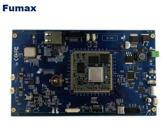
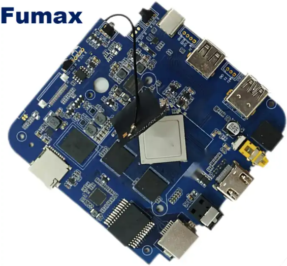
Shenzhen Fumax Technology Co., Ltd. is a company specializing in high-speed PCB design technical services, R&D prototypes, and small and medium-volume R&D and production services. Headquartered in Shenzhen, it has multiple SMT production lines, equipped with newly imported Fuji XPF, NXT3, AIMEXIII, fully automatic solder paste printing machine, ten/twelve temperature zone reflow oven, wave soldering and other high-end equipment, and equipped with AOI, 3DXRAY , 3DSPI, intelligent first article tester, fully automatic deboarding machine, BGA rework station, selective conformal paint and other equipment, focusing on high-quality R&D express, small and medium-sized batch SMT patching, assembly and other services.
How to query PCB bga packaging technology manufacturers?
To query the manufacturer of PCB BGA packaging technology, you can take the following methods:
- Search through the Internet: Enter the keyword “PCB BGA packaging technology manufacturer fumax” in the Google search engine to get relevant search results, including some well-known PCB BGA packaging technology manufacturers. You can learn about the manufacturer’s technical strength, product features, customer cases, etc. by browsing relevant websites.
- Industry exhibitions: By participating in relevant electronics exhibitions or industrial exhibitions, you can learn about some professional PCB BGA packaging technology manufacturers. By visiting the exhibition, you can communicate with manufacturer representatives and learn about the latest technology trends and product information.
- Industry associations: Join relevant electronics industry associations or organizations to obtain more industry information and resources. Through communication and sharing with association members, you can learn about some professional PCB BGA packaging technology manufacturers and establish cooperative relationships.
- Recommendation from friends or colleagues: You can consult friends or colleagues to learn about the PCB BGA packaging technology manufacturers they have used, and listen to their suggestions and opinions. In this way, you can find some reliable manufacturers and establish cooperative relationships.
In short, if you want to inquire about the manufacturers of PCB BGA packaging technology, you can search and learn about them through many ways. It is recommended to choose some well-known, professional and reliable manufacturers to cooperate with to ensure the quality and progress of the project.