To manufacture PCB boards for wireless chargers, you must first design the circuit diagram, then select the appropriate base material, such as FR4, CEM-1, etc., and prepare necessary materials such as components, solder, and flux.
When making the board, transfer the designed circuit diagram to the PCB board. Then use an automatic placement machine to mount the components on the PCB board, and connect the components to the PCB board through a welding process. Finally, testing and debugging are performed, and qualified PCB boards are packaged for transportation and delivery.
The industrial process of manufacturing PCB boards for wireless chargers can be divided into the following steps:
Design circuit diagram
Before manufacturing the PCB board of the wireless charger, you first need to design the circuit diagram. The circuit diagram is the basis for PCB board manufacturing. It includes all the components required for the wireless charger and the wires connecting these components. The design of circuit diagrams requires the use of professional circuit design software, such as Altium Designer, Eagle, etc. When designing a circuit diagram, it is necessary to select appropriate components and determine the connection relationship between them based on the functions and specifications of the wireless charger.
Prepare PCB board
After the circuit diagram design is completed, the PCB board needs to be prepared. PCB board is a substrate for installing components. It is made of insulating materials and has good mechanical strength and electrical properties. When preparing the PCB board, the size and layout of the PCB board need to be determined based on the arrangement and connection relationship of the components in the circuit diagram. At the same time, the appropriate material and thickness also need to be selected to meet the performance requirements of the wireless charger.
Making silk screen
On the PCB board, the arrangement and connection relationship of components need to be marked by silk screen printing. Silk screen is a thin line made of ink used to indicate the location and connection of components. When making screen printing, you need to use a screen printing machine to print ink onto the PCB board. The accuracy and clarity of the silk screen are crucial for subsequent welding and debugging, so they need to be made carefully.
Mounting of components
After making the silk screen, the components need to be mounted on the PCB board. The placement of components requires the use of a placement machine. The placement machine can accurately place components on the PCB board and ensure that their pins are aligned with the silk screen. During the placement process, placement speed and accuracy need to be strictly controlled to ensure the correct position and direction of components.
Welding
After the components are mounted, welding is required. Soldering is the process of connecting components to PCB boards, which includes spot welding and wave soldering. Spot welding refers to connecting solder points to component pins and PCB board wires to fix components and achieve electrical connections. Wave soldering refers to passing the PCB board through a molten solder tank so that the solder evenly covers the surface of the PCB board to achieve electrical connection between the components and the PCB board. During the welding process, the welding temperature and time need to be controlled to avoid damage to components and PCB boards. At the same time, the quality and reliability of welding need to be ensured to meet the performance requirements of the wireless charger.
Debugging and testing
After the welding is completed, the PCB board of the wireless charger needs to be debugged and tested. Debugging refers to the process of testing and adjusting the functions and performance of the wireless charger, and testing refers to the process of evaluating and testing the quality of the wireless charger. During the debugging process, each functional module needs to be tested to ensure that they can work properly. Overall testing is also required to check the overall performance and quality of the wireless charger. During the testing process, the appearance, size, electrical performance, etc. of the wireless chargers need to be tested to ensure that they meet the requirements.
Packaging and delivery
Finally, the PCB board of the wireless charger needs to be packaged and shipped. Packaging refers to the process of packaging and protecting wireless chargers and accessories to avoid damage during transportation. Shipping is the process of sending packaged products to customers. A final quality inspection is required before shipment to ensure that the product meets requirements. It also requires customized packaging and shipping processes based on customer needs and requirements.
In short, industrial manufacturing of PCB boards for wireless chargers requires multiple stages of precise operation and quality control to achieve a high-quality and efficient manufacturing process. It also requires continuous follow-up of technological innovation and management innovation to improve production efficiency and Reduce costs to meet market demands and development trends.
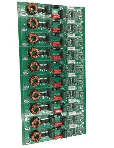
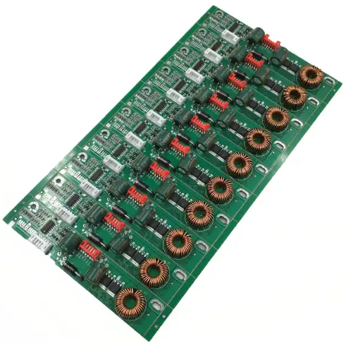
PCB board factory manufacturing wireless chargers
Fumax is a PCB board manufacturer specializing in wireless chargers. We have first-class equipment and technology to design and produce high-quality PCB boards. During the manufacturing process, we strictly control the material selection and process flow to ensure the reliability and performance of the PCB board.
In addition, we also provide one-stop services, including circuit design, board making, mounting, welding and testing, to meet customer needs for different types of wireless chargers. The factory has passed ISO9001 certification and has an experienced technical team to provide customers with a full range of technical support and solutions. No matter what type of wireless charger PCB board you need, our factory can provide you with high-quality products and excellent services.