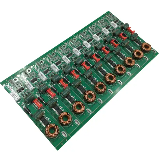
The PCB board wireless charger design and assembly process is a technology that assembles PCB boards and electronic components together. It mainly includes circuit design, PCB board manufacturing, component mounting, welding, testing and debugging.
During the assembly process, it is necessary to select appropriate materials and processes, such as high-precision PCB boards, soldering materials, flux, etc., to ensure product quality and reliability. At the same time, automated production line technology and digital management technology need to be adopted to improve production efficiency and management levels. Finally, through strict testing and debugging, it is ensured that the performance and quality of the product meet the requirements.
What other types of PCB boards are used in wireless chargers?
In addition to the wireless charger PCB boards mentioned above, there are many other types of PCB boards used by wireless chargers. Here are some possible other types:
- Magnetic wireless charger PCB board: This type of wireless charger uses magnetic materials to transmit power. They usually consist of a transmitter with a magnet and a receiver with a magnet. The design of the magnetic wireless charger PCB board needs to consider the design and optimization of the magnetic circuit to ensure efficient power transmission.
- Wireless power bank PCB board: This type of wireless charger is a portable device that can charge other devices. They usually consist of a battery and a small circuit board that can receive wireless power and store it in the battery, which then provides charging for other devices.
- Multi-device wireless charger PCB board: This type of wireless charger can charge multiple devices at the same time. They usually consist of a PCB board with multiple charging areas that can charge multiple devices at the same time. The design of the multi-device wireless charger PCB board needs to consider the location and charging needs of different devices to ensure efficient charging.
- Smart wireless charger PCB board: This type of wireless charger has intelligent functions that can automatically adjust charging parameters according to the charging needs and status of the device. They usually consist of a PCB board with control circuitry that monitors the device’s charging status and adjusts it as needed. The design of the smart wireless charger PCB board needs to consider the design and optimization of the control circuit to ensure efficient charging and device protection.
The PCB boards used by different types of wireless chargers have different characteristics and functions, and need to be designed and selected according to specific application scenarios and needs.
Can you introduce the first-class equipment and technology of wireless charger PCB board?
The first-class equipment and technology of wireless charger PCB boards include the following aspects:
- High-precision PCB manufacturing equipment: used to manufacture high-precision and high-reliability PCB boards, including CNC drilling machines, CNC milling machines, electroplating equipment, etc. These devices can ensure the accuracy and quality of PCB boards and meet the performance requirements of wireless chargers.
- SMT mounting equipment: used to mount electronic components onto PCB boards. These devices can automatically identify and place components, improving production efficiency and product quality.
- Welding equipment: used to connect components to PCB boards. These devices provide high-quality welding, ensuring the stability and reliability of electrical connections.
- Testing equipment: used to test the quality and performance of PCB boards. These devices can perform appearance inspection, electrical performance inspection, functional testing, etc. on PCB boards to ensure product quality and reliability.
- Automated production line technology: Through automated production line technology, various production links are connected to achieve efficient and automated production. This technology can improve production efficiency, reduce costs, and reduce the impact of human factors on product quality.
- Environmentally friendly production technology: With the improvement of environmental awareness, more and more manufacturers are adopting environmentally friendly production technologies, such as water-soluble flux, lead-free soldering, etc., to reduce the impact on the environment.
- Digital management technology: Through digital management technology, real-time monitoring and management of the production process can be achieved, and production efficiency and management levels can be improved.
First-class equipment and technology can improve the production efficiency and product quality of wireless charger PCB boards, meet customer needs, and promote the development of the industry.
How to introduce the raw material factory that manufactures wireless chargers?
The following is an introduction to the raw material factory that manufactures wireless chargers:
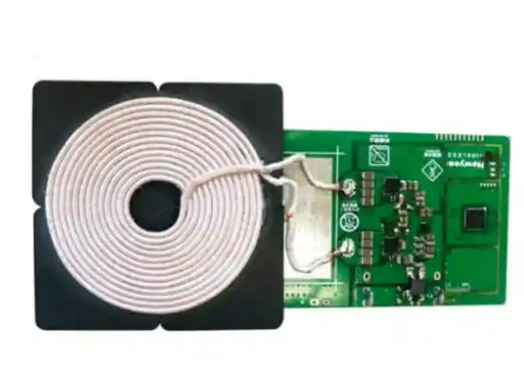
Welcome to our wireless charger raw material manufacturing factory. Here, we are committed to providing high-quality raw materials to wireless charging equipment manufacturers around the world, including but not limited to coils, batteries, magnetic materials, PCB boards and other key electronic components.
Shenzhen Fumax Technology Co., Ltd. provides diversified OEM and ODM services to domestic and foreign customers. We help customers solve operational problems such as mechanical or electronic design, sample and volume production, service and logistics, and more.
Our factory has advanced production equipment and first-class production lines, focusing on producing high-quality coils, which are the core components of wireless chargers. Our production lines feature automated and semi-automated coil winding, inspection and assembly capabilities, ensuring that each coil meets the highest quality standards.
At the same time, we also have a professional battery manufacturing workshop, focusing on the production of lithium batteries for wireless chargers. Our battery manufacturing equipment is advanced and our processes are mature, ensuring the stability and safety of our batteries.
In addition, we have advanced magnetic material production facilities. Magnetic materials are one of the key elements to achieve wireless charging. Our professional team produces magnetic materials with high magnetic permeability and low loss through precise processes and formulas.
Our factory also has a first-class PCB board manufacturing workshop, focusing on the production of PCB boards for wireless chargers. We have one-stop service capabilities from design to manufacturing to meet customers’ individual needs.
In order to ensure the quality and performance of each product, our production line adopts strict quality control processes, from the procurement of raw materials to the delivery of finished products, strict quality inspection is carried out in every link.
We are committed to providing customers with one-stop service. From product design, research and development to production and testing, we can provide you with professional support and efficient solutions. Our goal is to help you succeed in the wireless charger market.
Please visit our factory to learn more about our wireless charger raw material manufacturing. We look forward to working with you!