Switching power supply PCB design solutions are designed to achieve efficient and reliable power conversion while optimizing electromagnetic compatibility and thermal performance to meet various application needs.
- Switching power supply PCB design goals and requirements
- Switching power supply PCB schematic design
- Switching power supply PCB layout
- Switching power supply PCB wiring
- Switching power supply PCB post-processing
- Sorting and archiving of switching power supply PCB documents
- Switching power supply PCB design and assembly factory
The following is the framework and key points of a brief switching power supply PCB design solution for your reference:
Switching power supply PCB design goals and requirements
- Determine the power supply specifications and performance parameters, such as input voltage, output voltage, output current, efficiency, size, etc.
- Clarify design requirements, such as reliability, stability, EMC performance, thermal design, etc.
- Determine the PCB board material, number of layers, layout and wiring rules.
Switching power supply PCB schematic design
- Choose the appropriate power topology, such as BUCK, BOOST, BUCK-BOOST, etc.
- According to the circuit requirements, select appropriate electronic components, such as resistors, capacitors, inductors, diodes, MOSFETs, etc.
- Arrange the component layout reasonably according to the component data manual.
- Design a reasonable power circuit based on circuit requirements.
- Add necessary protection circuits, such as overcurrent protection, overvoltage protection, undervoltage protection, etc.
- Complete the schematic design and conduct simulation verification.
Switching power supply PCB layout
- According to the schematic diagram, plan the size and shape of the PCB board.
- Determine the principles of component layout, such as dividing according to functional areas, considering heat dissipation performance, etc.
- Perform special treatment on key components, such as adding heat sinks, mounting holes, etc.
- Consider EMC performance and reasonably arrange component spacing and location.
- Complete the preliminary layout design and conduct simulation verification.
Switching power supply PCB wiring
- Determine the wiring rules and line widths, such as the line width and spacing of power lines, ground lines, and signal lines.
- Carry out reasonable wiring planning based on the layout and schematic diagram.
- Follow the basic principles of wiring, such as avoiding loops and reducing crossovers.
- Perform special processing on key lines, such as thickening the line diameter, adding vias, etc.
- Consider EMC performance and arrange ground wires and other reference planes appropriately.
- Complete the wiring design and conduct simulation verification.
Switching power supply PCB post-processing
- Conduct inspections before PCB processing, such as DRC inspection, 3D view, etc.
- Add logos and comments as needed.
- Output PCB processing files, such as Gerber files, drilling files, etc.
- Complete PCB board making and component welding.
- Perform power supply performance testing and debugging.
- Conduct reliability testing and stability verification.
- Optimize and improve based on test results.
Sorting and archiving of switching power supply PCB documents
- Organize relevant documents in the design process, such as schematic diagrams, PCB layout, wiring files, etc.
- Write design specifications and user manuals.
- Archive and save design files to facilitate subsequent maintenance and improvement.
- Provide technical support and after-sales maintenance services in the project.
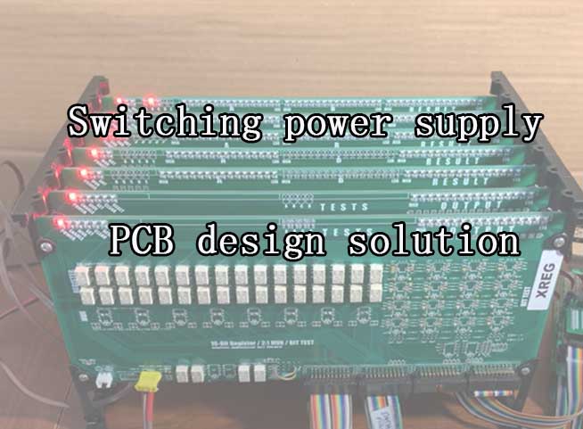
Switching power supply PCB design and assembly factory
Fumax switching power supply design PCB factory focuses on producing high-quality switching power supply PCB design, manufacturing, and assembly one-stop services, with advanced production equipment and a professional technical team.
We are committed to providing efficient and reliable power solutions to meet the needs of different fields. Our products are widely used in communications, medical, industrial control and other fields, and have won unanimous praise from customers.
We are committed to providing high-quality after-sales service and technical support to ensure customer satisfaction.