Multi-level HDI PCB design technology is an advanced printed circuit board (PCB) design technology, mainly used to implement high-density, high-performance electronic systems.
HDI PCB refers to High Density Interconnect PCB, which is a PCB technology that achieves high-density wiring in a small space.
Multi-stage HDI PCB design technology refers to designing HDI PCB into a multi-stage form to further improve the density and performance of the circuit.
Multi-level HDI PCB design technology analysis
The following is an analysis of multi-level HDI PCB design technology:
Advantages
(1) High-density wiring: Multi-stage HDI PCB design technology can achieve high-density wiring, making the circuit more compact and reducing the size and weight of the PCB.
(2) High performance: Multi-level HDI PCB design technology can achieve faster transmission speed and lower signal delay, improving the performance of electronic systems.
(3) Reliability: Multi-stage HDI PCB design technology uses advanced microvia and microstrip technology to make the circuit more reliable and reduce the possibility of failure.
(4) Flexibility: Multi-stage HDI PCB design technology can be customized according to actual needs to meet the needs of different electronic systems.
Design process
Multi-stage HDI PCB design technology needs to follow the following design process:
(1) Demand analysis: Conduct demand analysis based on actual needs to determine the function, performance, size and other requirements of the circuit.
(2) Scheme design: Based on the requirements analysis results, carry out scheme design, including circuit structure, wiring method, microvia and microstrip layout, etc.
(3) Layout design: Carry out layout design based on the scheme design results to determine the location and connection method of each component.
(4) Wiring design: Carry out wiring design based on the layout design results to achieve high-density, high-performance circuit wiring.
(5) Simulation test: After completing the wiring design, conduct simulation test to verify whether the function and performance of the circuit meet the requirements.
(6) Production: Based on the simulation test results, production is carried out to complete the production of multi-stage HDI PCB.
Key technologies:
The key technologies of multi-level HDI PCB design technology include microvia manufacturing technology, microstrip line manufacturing technology, high-density wiring technology, multi-layer stacking technology, etc. The application of these key technologies can improve circuit density and performance while ensuring circuit reliability and stability.
Application areas:
Multi-level HDI PCB design technology is widely used in communications, aerospace, medical electronics, automotive electronics and other fields. In these fields, the demand for high-density and high-performance circuits is increasing day by day, and the application of multi-level HDI PCB design technology is becoming more and more widespread.
In short, multi-level HDI PCB design technology is an advanced PCB design technology with the advantages of high-density wiring, high performance, reliability, flexibility, etc. With the development of electronic systems and the increase in demand, the application prospects of multi-level HDI PCB design technology will be broader.
What are the advantages of a multi-level HDI PCB design company?
The advantages of multi-stage HDI PCB design companies are mainly reflected in the following aspects:
- High-density wiring and high performance: Multi-level HDI PCB design technology can achieve high-density wiring and complex circuit design, thereby improving the performance and functionality of electronic products.
- Miniaturization and lightweight: Multi-level HDI PCB design technology can make electronic products miniaturized and lightweight through the use of high-density wiring and miniaturized components, making them easy to carry and use.
- Reliability: Multi-stage HDI PCB design technology uses advanced microvia and microstrip technology, which can improve the reliability and stability of the circuit and reduce the possibility of failure.
- High efficiency: Multi-stage HDI PCB design companies usually have professional design teams and advanced production equipment, which can quickly respond to customer needs and provide efficient design and production services.
- Personalized customization: Multi-stage HDI PCB design companies can carry out personalized customization according to customer needs to meet the special requirements of different electronic systems.
- Rich experience: Multi-stage HDI PCB design companies usually have rich design experience and good reputation, and can provide customers with high-quality design services and ensure product quality and performance.
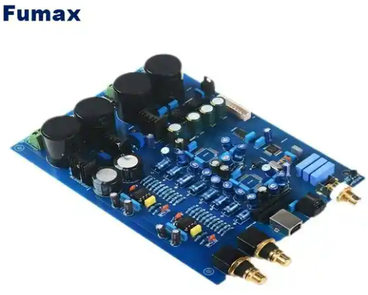
Fumax HDI PCB Manufacturer
Fumax multi-stage HDI PCB design company focuses on the design and development of high-density interconnection printed circuit boards and is committed to providing customers with excellent electronic system solutions. The company has a professional design team and advanced process technology, which can meet various high-density and high-performance circuit design needs.
Through continuous innovation and optimization, Multi-Level HDI PCB Design Company has become a leader in the industry, providing excellent electronic system design services to customers around the world.