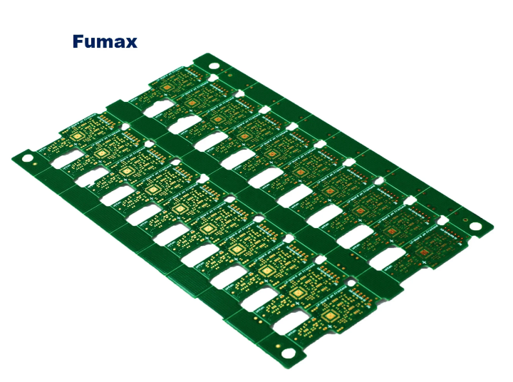
With the popularity of smart devices, wireless charging technology has become one of the essential functions of modern life.
As the core component to achieve this function, the importance of wireless charging PCBA (Printed Circuit Board Assembly) is self-evident. Below we will explain in detail all aspects of wireless charging PCBA to help you better understand this technology.
Overview of wireless charging PCBA
Wireless charging PCBA (Printed Circuit Board Assembly) is a printed circuit board assembly and is the core component of the wireless charging system. It integrates all electronic components and circuits required for wireless charging, including power transmission circuits, receiving coils, control circuits, power management circuits, etc. Through wireless charging PCBA, smart devices can realize wireless transmission of power and complete the charging process without directly contacting the charger.
Working principle of wireless charging PCBA
The working principle of wireless charging PCBA is based on the principle of electromagnetic induction. At the transmitting end, the oscillation circuit in the wireless charging PCBA generates a high-frequency alternating current, which generates a magnetic field through the receiving coil.

At the receiving end, the magnetic field energy is also received by the receiving coil and then converted into direct current to charge the battery. The entire process requires no physical connection, achieving efficient and convenient power transmission.
The composition of wireless charging PCBA
- Transmitter circuit: The transmitter circuit is the core part of the wireless charging system and is mainly responsible for generating high-frequency alternating current. It includes oscillation circuit, power amplifier circuit and full-bridge rectifier circuit. The oscillation circuit generates high-frequency alternating current, the power amplifier circuit amplifies the current to sufficient power, and the full-bridge rectifier circuit converts the high-frequency alternating current into direct current.
- Receiver circuit: The receiver circuit mainly includes the receiving coil, rectifier filter circuit and battery charging circuit. The receiving coil is responsible for receiving the magnetic field energy emitted by the transmitter and converting it into electrical energy. The rectifier and filter circuit converts the received AC power into DC power to provide stable power for battery charging. The battery charging circuit is responsible for controlling the battery charging process.
- Control circuit: The control circuit is the command center of the entire wireless charging system and is responsible for coordinating the work of various parts. It is mainly responsible for detecting charging status, controlling the charging process, adjusting charging power and other tasks. Control circuits are usually implemented using chips such as microcontrollers (MCU) or digital signal processors (DSP).
- Power management circuit: The power management circuit is mainly responsible for managing the power supply of the entire wireless charging system. It includes power switch, voltage regulator, overvoltage protection circuit and other parts. The power switch is used to control the power on and off, the voltage regulator is used to adjust the voltage, and the overvoltage protection circuit is used to protect the system from damage during overvoltage.
- Antenna: The antenna is an important component responsible for transmitting energy in the wireless charging system. It is usually made of magnetic materials that can effectively convert magnetic field energy into electrical energy or vice versa. The shape and size of the antenna have a great impact on wireless charging efficiency, so the design needs to be optimized based on the actual situation.
Application scenarios of wireless charging PCBA
Wireless charging PCBA is widely used in various smart devices, such as mobile phones, tablets, smart watches, etc.
By integrating the wireless charging PCBA into the device, users can charge the device at any time anywhere without having to worry about cable constraints and socket damage.
In addition, wireless charging also has the advantages of portability and ease of use, so it is favored by a large number of users.
The development trend of wireless charging PCBA
With the continuous advancement of technology and the continuous improvement of application requirements, the development trend of wireless charging PCBA is also constantly changing. In the future, wireless charging PCBA will develop in the direction of high performance, miniaturization, integration, safety and reliability.
At the same time, with the rapid development of emerging fields such as the Internet of Things and smart homes, the application scenarios of wireless charging PCBA will become more and more extensive, and its role in future smart life will be more important.
Summary: As the core component for realizing wireless charging function, wireless charging PCBA has wide application prospects and development space.
Understanding its working principle, composition and application scenarios will help to better understand this technology and provide useful references for future applications and development.